I. Core Causes of Inner Layer Residual Copper Shorts: A Full Process Breakdown
Before analyzing, let's first outline the basic workflow of inner layer pattern transfer:
Standard Process: Board Cutting (Routing) ➔ Baking ➔ Pre-treatment (Scrubbing/Micro-etching) ➔ Wet Film Coating / Dry Film Lamination ➔ Exposure ➔ Resting ➔ DES Line Routing ➔ Developing ➔ Acid Etching ➔ Stripping ➔ Washing & Drying ➔ Inner Layer AOI ➔ Inspection & Repair ➔ Lamination (Subsequent Process)
1. Inner Layer Pre-treatment: Poor Foundation Cleaning Buries Hidden Dangers
Pre-treatment is the first hurdle in inner layer manufacturing. Its core objective is to remove oil, oxidation layers, and impurities from the copper surface while ensuring the surface roughness meets standards, laying a solid foundation for subsequent pattern transfer.
- Copper Surface Adhesive Residue and Impurities: Incoming copper foil brings its own adhesive residue, and ink particles or dust remaining from the production process can adhere to the copper surface. This hinders the full reaction between the etching solution and the copper layer, resulting in localized incomplete etching that eventually turns into a residual copper short.
- Uneven Copper Surface Roughening: Uncontrolled scrubbing parameters (pressure, speed, brush grit) lead to the copper surface being either too rough or too smooth in localized areas. Excessive roughness easily causes dry film pinholes; excessive smoothness reduces dry film adhesion. Both cause pattern transfer deviations and trigger shorts.
- Board Bow and Twist Interference: The inner core board is usually quite thin. If warpage exceeds standards, it causes uneven contact between the board surface and the grinding wheels/spraying devices during pre-treatment, resulting in inadequate localized cleaning. It also destroys the alignment accuracy of subsequent exposure.
2. Inner Layer Pattern Transfer: Out-of-Control Exposure and Development are Disaster Zones
Pattern transfer is the critical link in accurately replicating the design layout onto the copper surface. It includes three major steps: lamination, exposure, and development. Any deviation will directly lead to residual copper adhesion.
A. Defects in the Exposure Stage
- Improper Exposure Energy:
- Insufficient energy ➔ Dry film is not fully polymerized and cured; after development, residual film shields the etching, forming residual copper.
- Excessive energy ➔ Dry film is "overexposed," trace edges are over-cured, and copper whiskers or bridges easily form during etching.
- Unclean Exposure Environment: Dry/wet film flakes floating in the exposure room or dust on the Film adhere to the dry film surface. After exposure and curing, they form an "invisible mask," preventing the corresponding copper area from being etched and creating a short.
- Alignment Deviation: Inaccurate alignment between the film and the board surface causes pattern misalignment and adjacent traces to overlap and stick. Core board warpage further exacerbates alignment errors, triggering batch shorts.
B. Defects in the Lamination Stage
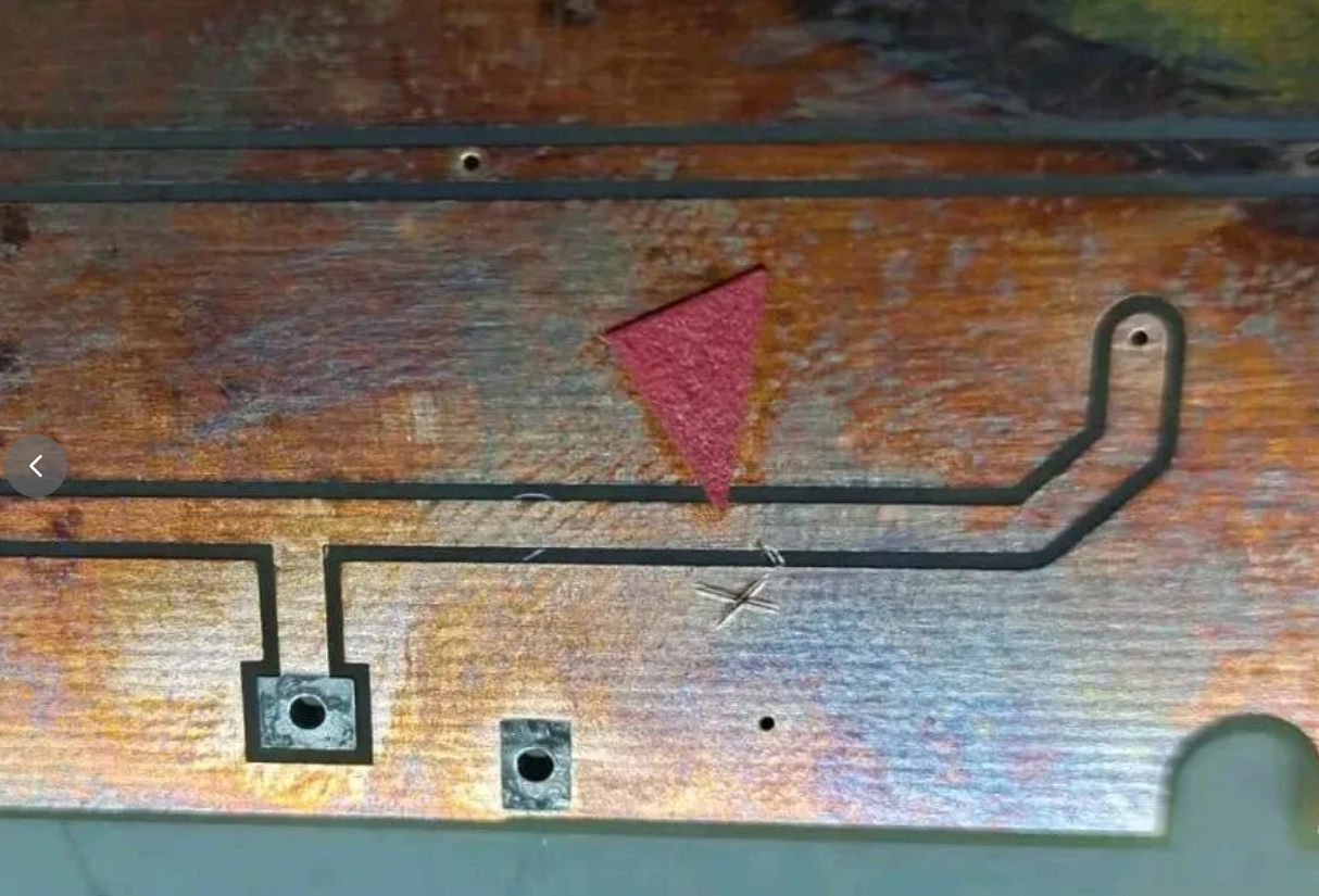
- Ink Slag Reverse Adhesion: During the coating/lamination process, residual ink slag and copper scrap from the equipment stick back onto the copper surface, covering parts of the trace area and hindering etching.
- Abnormal Dry Film Dimensions: If the dry film width is too large, dry film fragments generated during manual cutting adhere to the board surface and are not thoroughly removed after development.
- Improper Lamination Parameters: Mismatched temperature, pressure, and speed cause uneven bonding between the dry film and copper surface, leading to localized peeling or bubbles. The dry film falls off during etching, forming copper bridges between traces.
C. Defects in the Development Stage
- Incomplete Development: Insufficient developer concentration, low temperature, or excessive speed means the uncured dry film is not completely washed away and remains in the trace gaps.
- Dry Film Slag Reverse Adhesion: Detached dry film slag and copper slag in the developing tank adhere to the board surface. If cleaning is incomplete, they are carried into subsequent processes, creating a hidden danger for shorts.
- Dry Film Aging: Excessive dry film storage time or out-of-spec environmental temperature and humidity leads to performance degradation, causing uneven peeling and adhesive residue during development.

3. Inner Layer Etching: Failure of Chemical Bath and Equipment Control
A. Etching Solution Imbalance
- Excessive Copper Ion Concentration: Copper ions continuously dissolve and accumulate during the etching process. When the concentration exceeds 150g/L, the etching reaction rate drops significantly, and the copper in the trace gaps cannot be thoroughly dissolved.
- Insufficient Bath Activity: Low etching solution concentration, out-of-control temperature (e.g., below 45°C), or a pH value deviating from the optimal range leads to reduced etching capability.
- Etch Factor Imbalance: Excessive undercut causes the trace width to narrow, forming localized copper bridges; insufficient undercut fails to completely remove the copper layer between traces.
B. Equipment and Consumable Abnormalities
- Broken Filter: A damaged etching tank filter allows copper slag and impurities to flow back onto the board surface with the chemical solution.
- Clogged Nozzles / Uneven Spraying: Clogged nozzles lead to uneven spray pressure. The etching solution cannot fully contact localized areas, creating etching blind spots or the "Puddle Effect."
- Adhesive Slag Reverse Adhesion: Residual adhesive slag on the rollers and conveyor belts of the etching equipment adheres to the board surface, covering copper areas.
4. Inner Layer AOI and Repair: Missed Inspections and Improper Repairs
Inner Layer Automated Optical Inspection (AOI) is the last line of defense to intercept defects before they enter the lamination process.
- AOI Missed Inspections: Delayed calibration of equipment optical parameters or light source attenuation prevents micro-level residual copper, copper whiskers, and other tiny defects from being identified.
- Incomplete Repair / Manual Repair Defects: When manually repairing defects marked by AOI, failing to thoroughly scrape off residual copper or generating new copper scrap impurities during the repair process; non-standard operations cause traces to lift, triggering secondary short-circuit risks.
5. Handling Operations: Potential Risks of Foreign Object and Spacer Contamination
- Spacer and Film Contamination: Copper scrap and dust remain on the surface of the films used for spacers. If put online without thorough cleaning, the copper scrap is pressed into the inner trace gaps before lamination.
- Logistics Turnover Contamination: Copper scrap and ink slag remaining on turnover trays and fixtures adhere to the inner layer board surface. (This type of reverse adhesion caused by handling is often the easiest to overlook on the shop floor.)
II. Inner Layer Residual Copper Shorts: Systemic Improvement Countermeasures
1. Pre-treatment Process: Build a Solid Foundation Cleaning Defense Line
- Incoming Material and Process Cleaning Control: Establish incoming inspection standards for copper foil, focusing on spot-checking for adhesive residue and impurities. Pre-treatment stations should be equipped with high-efficiency dust removal devices. Regularly clean coating and lamination equipment to eliminate reverse adhesion of ink slag and copper scrap.
- Precise Parameter Control: Optimize scrubbing parameters (pressure 0.3-0.5MPa, speed 1.5-2.0m/min) and regularly test copper surface roughness (Ra 1.0-1.5μm). Establish a core board warpage testing standard; boards with warpage >0.5% are prohibited from entering pre-treatment.
- Regular Equipment Maintenance: Clean pre-treatment spray devices and rollers daily, and dismantle and clean the scrubbing machine weekly to ensure no adhesive slag and impurities remain.
2. Pattern Transfer Process: Strictly Control Exposure and Development Accuracy
- Refined Control of the Exposure Stage:
- Energy Calibration: Calibrate exposure energy daily using an exposure scale or energy meter (adjusted based on dry film type, usually 80-120mJ/cm²).
- Environment and Alignment: Maintain exposure room cleanliness at Class 1000 or above. Adopt a high-precision alignment system, and add a preheating and leveling process to combat board warpage. Thoroughly clean the film/LDI light table before use.
- Standardized Lamination Operations: Regularly clean coating equipment and replace aging ink. Strictly control lamination parameters (temperature 110±5°C, pressure 0.4-0.6MPa, speed 2.0-2.5m/min) and avoid generating fragments from manual film cutting.
- Zero-Defect Development Control:
- Establish a real-time monitoring system for developer concentration and temperature (concentration 1.0-1.2%, temperature 30±2°C), and regularly replace developer tank filter cartridges.
- Specialized Tank Cleaning Agent: Use specialized tank cleaning agents to comprehensively clean the dead corners of the developing tank.
- Note: It is strictly prohibited to develop dry film and wet film on the same line to avoid cross-contamination of residues.
3. Etching Process: Implement Dual Closed-Loop Control for Chemicals and Equipment
- Precise Etching Solution Management: Introduce a closed-loop control system to monitor copper ion concentration in real-time (control at 120-150g/L) and automatically replenish the etching solution. Ensure temperature (45-50°C) and pH value (0.8-1.2) are in the optimal range.
- Full Lifecycle Equipment Maintenance: Inspect filter integrity daily. Clean nozzles and spray pipelines weekly to ensure uniform spraying (pressure 0.2-0.3MPa). Regularly maintain rollers and conveyor belts.
- Etch Factor Optimization: For high-end fine lines (≤50/50μm), it is recommended to adopt vacuum two-fluid etching technology to improve the etch factor, control the undercut to ≤10μm, and ensure etching uniformity reaches 95% or more, fundamentally avoiding copper bridges or residual copper.
4. Inspection and Repair Process: Construct a Full-Process Interception System
- AOI Equipment Performance Improvement: Calibrate AOI optical parameters and light sources every half month to ensure a minimum defect recognition capability of ≤5μm. Increase the scanning magnification for high-density trace areas to prevent missed inspections.
- Standardized Repair Operations: Formulate an AOI inspection and repair Standard Operating Procedure (SOP). Use high-precision tools to thoroughly remove residual copper and re-inspect under a microscope. Gradually reduce reliance on manual repair and prioritize the introduction of automated repair equipment.
5. Standardized Handling Operations: Eliminate Foreign Object Contamination
- Film Cleaning Control: Before use, spacers must be thoroughly wiped with a lint-free cloth and special cleaning agent. Regularly replace aging films, and require all films to undergo a deep cleaning "once a month."
- Turnover Environment Optimization: Comprehensively use anti-static dust-free turnover trays. Clean fixtures and workbenches daily. Enforce personnel regulations, ensuring they wear dust-free gloves and masks to avoid manual contact contaminating the board surface.
III. Conclusion
Inner layer residual copper shorts are a complex defect resulting from "multiple overlapping factors." Their control must run through the entire process—including pre-treatment, lamination, exposure, development, etching, AOI inspection, and logistics handling. An oversight in any single link will cause the defect to be infinitely magnified.
Although there are many causes, the key points of failure are usually limited to one or two areas; a comprehensive loss of control is highly unlikely in practice. Factories can accurately pinpoint the Root Cause of residual copper shorts through engineering methods such as defect appearance judgment, Cross-section analysis, cross-comparison verification, step-by-step elimination, and Design of Experiments (DOE).
As the demand for PCB precision driven by AI computing power continues to climb, advanced technologies such as LDI (Laser Direct Imaging), supercritical CO₂ cleaning, vacuum two-fluid etching, and AI intelligent parameter adjustment will become the keys to breaking through yield bottlenecks. Excellent equipment paired with a rigorous control system is what ultimately delivers outstanding final process yields!
