April 28, 2026
A multilayer PCB is primarily composed of two critical materials: the Core and the Prepreg (PP).
Manufacturing Insight: During fabrication, it is generally recommended not to stack more than three sheets of Prepreg in a single dielectric layer (typically keeping the thickness around 20 mils). Because Prepreg is in a semi-solid state and flows during pressing, the final pressed thickness will have some tolerance. This physical variation is a primary reason why achieving absolute consistency in Impedance Control can be challenging.
Copper foil thickness is standardly measured in ounces (oz). In the PCB industry, 1 oz of copper means that 1 ounce (28.35g) of copper is spread evenly over one square foot of area. This equates to a thickness of 1.37 mils (often rounded to 1.4 mils or 35 µm).
The two main types of copper foil used are:
The choice of dielectric material directly impacts both electrical performance and mechanical integrity.
Advanced Materials for High-Speed and Environmental Compliance:
When designing for signal integrity (SI) in high-speed or high-frequency applications (like AI servers or Co-Packaged Optics), the standard FR4 is often insufficient. Engineers must select materials with a lower Dielectric Constant (Dk) to increase signal propagation speed, and a lower Dissipation Factor (Df) to minimize dielectric loss.
High-end substrate families from manufacturers like Panasonic (MEGTRON series), Rogers, TUC, and Isola are frequently utilized for these demanding designs. Furthermore, environmental regulations often dictate material choice. When strict Halogen-Free compliance is required, it is critical to specify the exact material grade—for example, upgrading from a standard KB-6164F to KB-6165G to ensure the board meets all environmental thresholds without compromising electrical performance.
Standard impedance requirements typically include 50Ω single-ended, 100Ω differential, and 50Ω RF lines.
RF traces require strict 50Ω control and are usually routed on the top or bottom surface layers. This microstrip topology allows for direct component connection without vias, eliminating impedance discontinuities while leveraging faster surface propagation speeds. To minimize loss and improve immunity, RF traces are wider (often 15 mils or more).
To maintain a 50Ω impedance with a wider trace, the distance to the reference plane must increase. Therefore, surface RF lines often reference the third layer, requiring a calculated anti-pad (copper keep-out) on the second layer directly beneath the RF trace.
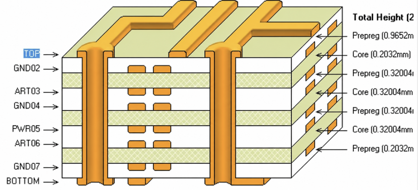
In many organizations, Schematic capture and PCB Layout are handled by different engineers. However, Hardware Engineers must understand stack-up construction to effectively guide the Layout team and review the final design.
While common consumer boards use 6, 8, or 12 layers, complex designs easily exceed 16 layers. Balancing cost and manufacturability is key; for example, a high-density 16-layer HDI project can often be optimized from an expensive "Any-layer" build down to a highly reliable 4-lamination cycle construction.
When reviewing a layout, apply these fundamental principles to ensure Signal and Power Integrity (SI/PI):
Power and Ground planes should be as close as possible, ideally adjacent. This creates a large inter-plane capacitance, acting as a natural decoupling capacitor and lowering the Power Delivery Network (PDN) impedance. If a power layer is heavily fragmented by multiple voltage rails, placing it immediately adjacent to a solid Ground plane is critical.
High-speed signals must route adjacent to a continuous, solid reference plane (either Power or Ground) to ensure a continuous return path. Never route high-speed signals across split planes, as this forces the return current to take a longer, higher-impedance path, causing severe EMI and signal degradation.
Routing signals on two directly adjacent layers drastically increases crosstalk. If stack-up limitations force adjacent signal layers, they must be routed orthogonally (one layer routed strictly horizontally, the other vertically) to minimize coupling.

