May 22, 2026
When PCB engineers are laying out a new product, their work goes far beyond simply connecting traces on the outer layers; the design of the power and ground planes on the inner layers is actually even more critical. When working on the inner layers, engineers must not only take a comprehensive approach to power integrity (PI), signal integrity (SI), and electromagnetic compatibility (EMC), but they must also ensure that “design for manufacturability (DFM)” is not overlooked. The outer layers of a PCB are primarily used for routing traces and soldering components, while the inner layers are used to route power and ground paths (applicable only to multilayer boards). When we refer to two-layer, four-layer, or six-layer boards, we are referring to the total number of signal layers and inner power/ground layers.
Placing a solid ground plane directly beneath critical signals (such as high-speed signals, clock signals, and high-frequency signals) ensures the shortest return path for the signal and minimizes radiation.
In high-speed circuit design, it is essential to properly handle the interference caused by power supply radiation to the entire system. The general principle is: the area of the power plane should be smaller than that of the ground plane, using the ground layer to shield power supply interference. The industry-standard 20H Rule recommends shrinking the power plane by 2 times the dielectric thickness relative to the ground plane.
Adjacent power and ground layers should be placed as close together as possible. The goal is to create interlayer coupling capacitance, which works together with the decoupling capacitors on the board to lower the impedance of the power plane and achieve broader filtering performance.
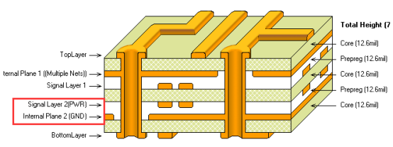
The choice of reference layer is crucial. In theory, both power and ground layers can serve as reference layers. However, because the ground layer is typically connected directly to the chassis or earth, its shielding effectiveness is far superior to that of a power layer. Therefore, the design should “prioritize the ground plane” as the signal reference layer.
Critical signals on adjacent layers must absolutely not cross a split in the reference plane. Crossing a split forces the return current to take a detour, creating a large signal loop area that generates strong radiation and crosstalk.

To maintain the integrity of the ground plane, it is strongly recommended not to route signals on ground layers. If signal density is extremely high and unavoidable, consider routing on the edge of a power layer.
PCB manufacturing is a highly complex chemical and physical process, and inner layer production is just one part of it. When fabricating inner layers, tolerances of downstream processes (such as lamination and drilling) must be taken into account, as they directly affect inner layer yield and quality. For multilayer boards, the process is much more complex than for single or double‑sided boards, so a DFM mindset is essential during design.
An independent pad refers to a via pad on an inner layer that is not connected to any net. During PCB CAM processing, board houses typically remove these non‑functional pads. Keeping them does not help the circuit function, wastes valuable routing space, and increases drill bit wear during drilling, affecting quality and production efficiency.

BGA components are small and have extremely dense pin counts, resulting in very dense fan‑out vias. During manufacturing, sufficient clearance must be maintained between the drill hole edge and adjacent traces or copper; otherwise, slight misalignment during lamination or drilling can cause shorts.
However, to maintain safe clearances, the copper between closely spaced vias may become overly thinned or even break, causing an open circuit. Therefore, when CAM engineers handle BGA regions and find that copper between vias has been broken, they must manually add a “copper bridge” to ensure correct connectivity in mass production.
Sometimes a design uses a negative layer, but all holes have a solder mask ring. When viewed as a positive image, this means that all holes are completely isolated from the copper foil and not connected to any net. Such a “fully isolated” condition renders the inner layer functionally useless.
When a board house encounters this issue, it will certainly issue an Engineering Question (EQ) to the R&D engineer. This is usually a design oversight caused by forgetting to assign net attributes when pouring copper.
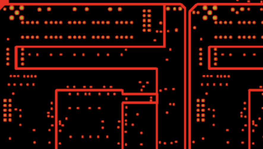
When splitting power or ground planes on inner layers, overly dense vias can create narrow conductive necks on the copper foil (commonly called the “Swiss Cheese Effect”). If the copper bridge width for a power net is insufficient, it cannot carry the expected current – leading to excessive voltage drop in mild cases or direct burnout in severe cases. In extreme situations, the neck may even fracture and open, resulting in product design failure.
All the manufacturing risks mentioned above can be identified by professional DFM software during the design phase. As a hardware engineer, it is strongly recommended to run a DFM check before releasing the board for fabrication. Detecting issues early – such as overly narrow copper bridges, unremoved non‑functional pads, or incorrect negative layer net assignments – and fixing them in the layout phase will not only prevent production delays but also significantly improve the first‑pass success rate of NPI prototypes, saving the company considerable trial‑and‑iteration costs.
