October 5, 2026
When a rigid PCB will not fit inside the enclosure and a cable assembly introduces unwanted connector risk, a rigid-flex PCB may appear to be the obvious solution. It integrates rigid circuit sections and bendable interconnects
This is the first condition to define.
A flex-to-install circuit is bent a limited number of times during assembly and remains in a fixed shape afterward. A dynamic-flex circuit moves repeatedly during operation, as in a sliding module, robotic arm, or movable sensor.
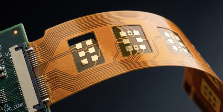 These applications require different decisions regarding copper, layer count, bend radius, and trace arrangement. If the drawing only states that an area is flexible but does not define direction, angle, cycle count, and operating environment, the fabricator cannot fully evaluate copper-fatigue risk.
The design input should include at least:
When a flex circuit bends, the outer material is stretched while the inner material is compressed. An excessively small radius can cause trace cracking, copper fatigue, coverlay separation, or intermittent opens after repeated use.
Common rules expressed as a multiple of board thickness are suitable only for early estimation. The acceptable bend radius also depends on flex thickness, layer count, copper thickness, copper type, adhesive system, bend direction, and number of cycles.
The mechanical drawing should show the actual installed shape, not only the flattened circuit. This allows the team to identify whether the flex section is being pulled tight, sharply folded, or compressed by enclosure features.
A conventional rigid-board layout focuses mainly on electrical connectivity and manufacturing clearance. Flex traces must also withstand mechanical strain.
Where practical, avoid the following inside active bend areas:
Traces generally use smooth geometry through a bend area, with copper distributed as evenly as practical. Connections to larger copper features should also avoid sharp corners and sudden width transitions.
The objective is to reduce local stress concentration, not to impose a universal pattern. The final arrangement must still reflect layer count, trace width, copper thickness, and bend direction.
The rigid-to-flex transition contains simultaneous changes in material, thickness, and stiffness, making it a natural stress-concentration area.
If vias, pads, components, or stiffener edges are positioned too close to the transition, loads introduced during assembly, handling, or use may be transferred into via barrels and solder joints. Sharp internal corners or notches can also concentrate stress.
The design review should confirm:
There is no single clearance value suitable for every fabricator. The final structure must be confirmed against the selected materials, thickness, layer count, and process capability.
Polyimide, or PI, is a common flex-circuit material, but specifying PI alone does not define the construction.
A complete material and stackup definition may include:
A copper system suited to repeated deformation is commonly considered for dynamic-flex applications, but material naming alone cannot determine service life. Copper thickness, plating, trace orientation, bend radius, and cycle count all contribute to the result.
A rigid-flex PCB may eliminate some connector transitions, but its signal path can still contain impedance discontinuities.
A high-speed signal may pass through a rigid region, layer transition, rigid-to-flex transition, and flex region. Dielectric thickness, dielectric constant, copper thickness, and reference-plane structure may differ between these areas, so they must be evaluated using the production stackup.
Review whether:
Removing copper to improve flexibility may also alter the signal return path. Mechanical design, PCB layout, and impedance modeling must therefore use the same structural assumptions.
Stiffeners are commonly placed under connectors, soldering areas, or contact regions that require local rigidity. A larger stiffener is not automatically safer; an edge positioned at a bend or load point may create a new stress concentration.
Assembly planning should also consider:
If these questions are postponed until the PCB is complete, fixtures alone may no longer solve the underlying problem.
| Information | What to define | | :--- | :--- | | Stackup drawing | Materials, layers, copper, and dielectric thickness in rigid and flex regions | | Bend drawing | Location, direction, angle, radius, and number of movements | | Mechanical drawing | Installed shape, movement envelope, and load direction | | Material list | Base material, copper, coverlay, bonding material, and stiffeners | | Impedance table | Signal layer, reference layer, target impedance, and operating band | | Assembly information | Reflow process, carriers, connectors, and handling restrictions | | Operating environment | Temperature, humidity, vibration, and expected use |
Before release, confirm that:
A rigid-flex PCB does more than integrate wiring into a circuit board. It combines electrical interconnection and mechanical movement in one design.
Reliability depends less on whether the design “uses PI” and more on whether its bending conditions are clearly defined, its stackup is appropriate, stress is kept away from vulnerable circuit features, and signal and assembly requirements are evaluated against the same mechanical conditions.
When planning a flex or rigid-flex PCB, prepare the Gerber data, preliminary stackup, mechanical drawing, bending conditions, and impedance requirements. eCloud can help organize the engineering conditions that need confirmation before release, allowing questions to be raised while the structure can still be adjusted rather than after trial production reveals cracked traces, impedance deviations, or assembly interference.
