July 4, 2026
As AI servers, automotive electronics, 5G/Wi-Fi 7, and edge AI become ubiquitous, EMI/EMC has shifted from a "compliance hurdle" to a determining factor for whether a product can ship in volume. A board that runs cleanly on the bench can show up at the EMC lab with a +15 dB spike at 200 MHz — and the first instinct is usually to add a shield can or absorber sheet. But the root cause is almost always buried in the stackup and routing decisions made weeks earlier. This article walks through 7 PCB EMI/EMC design principles and explains why stackup and return paths — not shielding — are what actually decide compliance.
EMI is, at its core, electromagnetic energy leaking from one circuit to another. There are two leakage paths: radiation through the air (radiated emission) or conduction through cables (conducted emission). External noise enters the system through the same two paths. EMI is most problematic between 9 kHz and 6 GHz – above that, interference typically stays within a single board and falls into the signal integrity (SI) category instead.
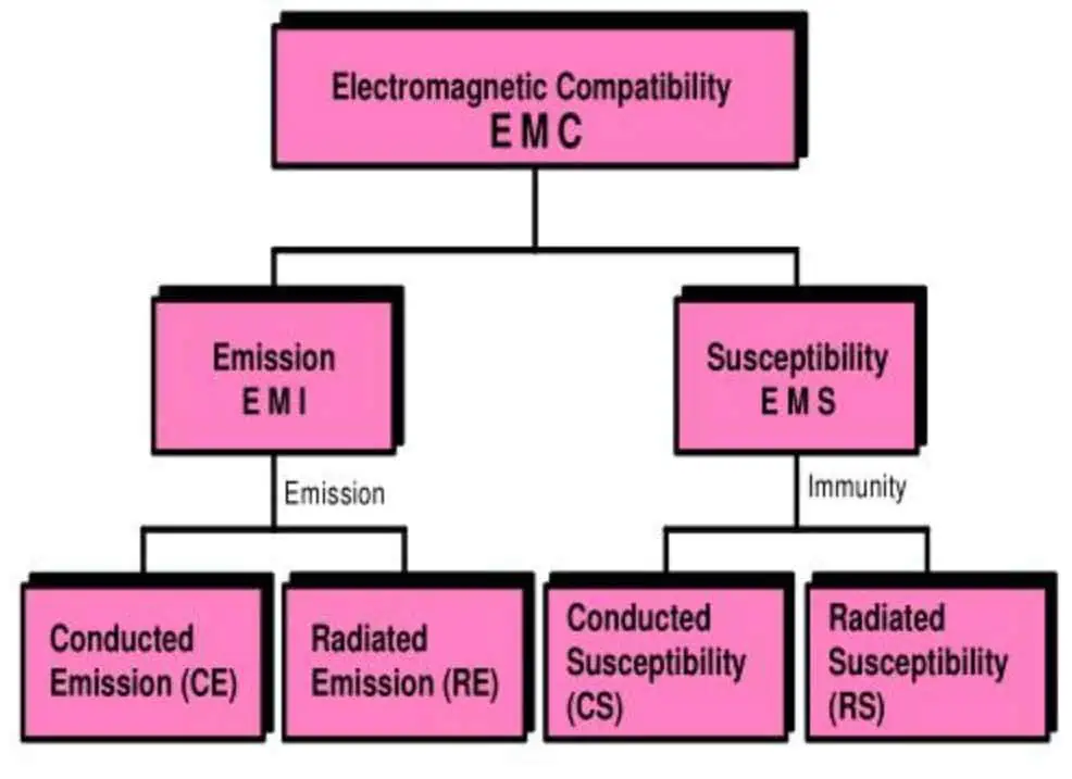 EMC (electromagnetic compatibility) is the flip side: in a regulated environment, the board must neither emit excessive noise nor be susceptible to external interference. Common EMI sources are summarised below:
| Type | Source | Mechanism | | :--- | :--- | :--- | | High‑speed switching | Digital clocks, SMPS, DC‑DC, PWM | Fast rise/fall edges produce high‑frequency harmonics | | Cable radiation | Unshielded cables, ribbon cables | Length approaches λ/4, becomes a resonant antenna | | Trace radiation | Long, unterminated high‑speed traces | Trace itself becomes a radiating antenna | | Plane defects | Split grounds, enclosure seams | Slot approaches λ/2, becomes a slot antenna | | Floating conductors | Unterminated IC pins, test pads, heatsinks | Any floating metal acts as an antenna | | Insufficient decoupling | Missing or misplaced decoupling caps | High‑frequency noise reaches the power rail |
The common pattern is clear: any “rapidly changing current or voltage” combined with an “uncontrolled loop” will radiate. All 7 principles below are about solving these two things.
Stackup is the first watershed for EMC. Every signal layer must have an adjacent solid reference plane (ground or power) – this is the most non‑negotiable rule.
Many EMC failures trace back to 2‑ or 4‑layer boards being pushed into high‑speed designs without adjacent reference planes for every signal. Stackup decisions have far greater impact than adding shield cans later.
Choosing the right transmission line structure is the second gate to keeping traces from becoming antennas.
For 224G PAM4 and PCIe 6.0 designs, stripline paired with HVLP copper foil and M8/M9‑grade CCL has become the default – precisely because of stripline's superior field containment over microstrip.
Every signal forms a loop with its return path on the reference plane – and the larger the loop, the stronger the radiation. Controlling loop area is the lowest‑cost, highest‑leverage decision in EMC design.
The most common violation in practice is “letting the clock trace meander across the board for layout aesthetics.” An extra 1 cm of trace seems harmless, but at 1 GHz harmonics (λ ≈ 30 cm in air), doubling loop area can raise radiated emissions by 6 dB.
When a signal changes layers through a via, the return path is broken – unless explicitly bridged.
The blind spot here is treating stitching vias as decoration. Without calculating spacing based on frequency and the actual transition geometry, the effect is limited.
Once stackup, loops, and return paths are sorted, the final line of defence is edge control – managing energy entering and leaving the board.
Order matters – filtering handles conduction, shielding handles radiation, and they typically work together. Jumping to shielding before fixing stackup and loops is like patching a leak after the water has flooded the room: expensive and only partially effective.
Boards that fail EMC usually fail because of stackup and routing decisions, not because they were “under‑shielded.” A 4‑layer board running a 1 GHz clock with an unplanned return path and floating outer copper pour cannot be saved by any amount of ferrite beads, shield cans, or absorbers added later. FCC Part 15, CISPR 11, and MIL‑STD‑461 define test thresholds – they are not design guides. What actually gets a board through certification on the first attempt is calculating fields, loops, and frequency bands at the design stage.
In our DFM reviews, three EMC risks come up most often:
eCloud provides integrated prototyping and production for HDI and multilayer high‑speed boards, with extensive EMC design experience across AI acceleration, high‑speed networking, automotive, and silicon photonics applications. Planning a high‑speed project? Talk to our engineering team during layout – get stackup, impedance, and EMC‑related DFM feedback early, so you don't discover at the EMC lab that the board needs to be re‑laid out.
