June 5, 2026
In PCB design, mastering solder mask clearance isn't just a minor detailing task—it is a make-or-break factor for SMT assembly quality. Solder mask clearance (the spacing between the copper pad and the surrounding mask) typically ranges from 2 to 7 mils. Whether you are placing a fine-pitch BGA, a standard IC, or basic passives, each component profile demands specific clearance rules. For hardware R&D and layout engineers, locking down these parameters during the design phase is the best way to sidestep costly DFM nightmares like solder bridging, mask peeling, or registration shifts. Here is a deep dive into why these tolerances matter, along with practical guidelines for different component types.
Solder mask clearance (or expansion) dictates exactly how much of your copper pad is exposed. It requires calculating a precise balance between your component's footprint, its pitch, and your manufacturer’s registration capabilities.
You cannot just guess these numbers. You have to walk a fine line between electrical safety and fabrication limits:
If the distance between two pads is smaller than your fabricator's minimum solder mask dam/web capability (usually 4 to 7 mils), the safest route is to use a "gang mask" (block clearance) , which merges the openings to prevent manufacturing defects.
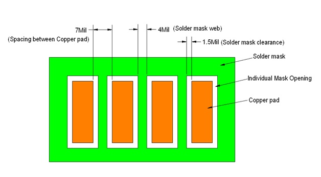
The ideal clearance depends heavily on pad size, pitch, and your PCB supplier's alignment tolerances. Here are the recommended baseline values:
Standard clearance typically ranges from 2 to 6 mils per side.
💡 Pro‑Tip: If your pitch is under 0.5 mm, verify that your fab can reliably print a 3‑mil mask web. If they cannot, switch to a gang mask layout.
BGAs are notoriously unforgiving. Even a slight mask misregistration can ruin solder ball landing and joint reliability.
💡 Pro‑Tip: For ultra‑micro BGAs (pitch <0.4 mm), you might need to use Solder Mask Defined (SMD) pads due to spatial limits. However, Non‑Solder Mask Defined (NSMD) pads are generally preferred for better mechanical joint strength.
Clearances here vary based on physical size and required solder volume (usually 2 to 8 mils).
These components endure mechanical stress during plugging or vibration. Aim for a 3 to 8 mil clearance. It is highly recommended to increase the mask pullback around mounting holes and anchor pads to prevent the mask from cracking or flaking off.
These require larger clearances to absorb thermal and mechanical stress during operation and soldering. DIP pin perimeters generally need a 4 to 6 mil pullback. For high‑current loads, ensure the mask does not overlap heavily with large copper pours to prevent localised delamination.
Want reliable joints without the shorts? Keep these rules in mind:
Adding clear mask instructions to your Fab Notes saves everyone time and prevents CAM engineers from guessing your intent. Include these points:
Dialling in the right solder mask clearance is fundamental for R&D engineers who want to avoid SMT shorts and guarantee high PCBA yields. However, navigating the intricate DFM limits of different manufacturing environments on a tight development schedule is exhausting.
As a service‑oriented digital integrator and engineering specialty platform, eCloud Technology understands the friction R&D teams face. We are not a traditional factory; we are your ultimate engineering backend. The next time you are prepping a complex board for prototyping, let the eCloud team take the wheel. We leverage our deep engineering expertise to validate your design constraints, ensuring a flawless, seamless transition from layout directly to successful SMT assembly!
