April 30, 2026
As an enterprise focused on advanced Printed Circuit Board (PCB) manufacturing, the global engineering team at eCloud Technology is dedicated to engaging throughout the entire product lifecycle. From upfront R&D and prototyping to final mass production, we provide a one-stop technical solution to ensure every delivery meets our customers' stringent demands for high quality and reliability. Today, we want to share "5 Cost-Saving PCB Design Practices" summarized by eCloud's senior engineering team. Through these Design for Manufacturability (DFM) perspectives, we hope to help you avoid potential pitfalls early in the R&D phase, creating a perfect product that balances performance and cost.
Our goal is to help customers design exceptional PCBs. This means advocating for deep cross-functional collaboration—from procurement and QA to application and process engineering teams—at the very beginning of a project.
In hardware development, we strongly oppose "Watermelon Projects"—projects that look green (on track) on the outside but are full of unresolved manufacturing risks (red) on the inside. While upfront DFM reviews may seem time-consuming, they drastically reduce rework costs later on. Before starting your layout, be sure to confirm these 6 key questions with your team:
Once you have defined the most complex core of your design, simplify the rest as much as possible. The simpler the PCB manufacturing process, the higher the production yield. This not only saves money and time but also accelerates your New Product Introduction (NPI) time‑to‑market.
For example, when planning an HDI stack‑up for high‑end servers or networking products, don't blindly chase the highest specs. Often, a well‑planned 16‑layer HDI board using a 4‑lamination cycle structure can perfectly meet signal and routing demands, completely eliminating the need for astronomically expensive "Any‑layer" HDI processes.
"A designer knows he has achieved perfection not when there is nothing left to add, but when there is nothing left to take away." — Antoine de Saint‑Exupéry, The Little Prince
Once your primary electrical attributes are established, ensure your PCB's technical requirements align with the manufacturing facility's capabilities.
Different applications (e.g., heavy copper, RF, HDI, Rigid‑Flex) require entirely different equipment and process know‑how. More importantly, material selection is critical:
Ensure your engineers and manufacturing partners use a common material library and process standard from prototype to mass production to prevent impedance or reliability shifts when moving between facilities.
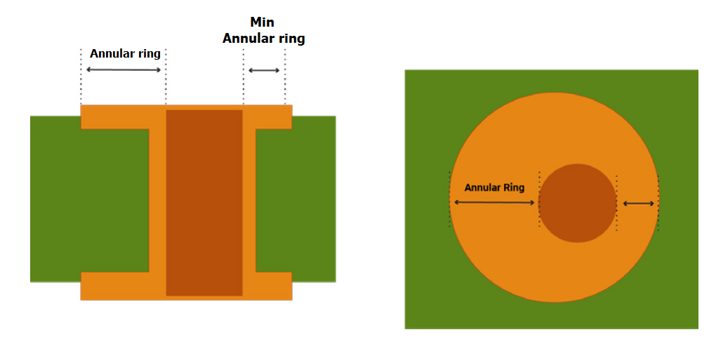
Build physical variation allowances into your design. On the factory floor, the most common DFM roadblock is "insufficient space," and the most fatal flaw is usually the Annular Ring.
Drilling machines have mechanical tolerances, and lamination processes have layer‑to‑layer misregistration. Whenever possible, increase the annular ring size for vias, or slightly relax the trace/space rules in non‑critical areas. Leaving adequate process tolerances makes production smoother for the fab, and prevents you from paying higher unit prices due to low yields.
PCB cost calculations are primarily based on the utilization of the "Working Panel." Even though standard industry panel sizes are typically 18” × 24” or 21” × 24”, be sure to discuss your array layout with eCloud's engineers.
Sometimes, tweaking a board dimension by just 2‑3 mm or altering the V‑Cut and routing paths allows an 18" × 24" panel to fit several more arrays—directly dropping the manufacturing cost of a single PCB by over 10%!

eCloud Technology focuses on advanced PCB manufacturing technologies, committed to providing our customers with seamless technical services. From demanding thermal solutions and high‑frequency microwave boards to high‑end microvia HDI, our products are widely used in telecommunications, industrial control, automotive electronics, and advanced computing markets.
Running into bottlenecks with stack‑up or material selection? Reach out to eCloud's experienced Field Application Engineers (FAE) today to get customized technical consulting and a quote for your next prototype!
