June 26, 2026
As wireless communication pushes from Sub-6 GHz all the way to mmWave, coupled with the comprehensive takeoff of AI infrastructure, automotive radar, low-Earth orbit (LEO) satellites, and Wi-Fi 7, RF and microwave PCB design is no longer the exclusive domain of a few specialized RF engineers. Today, as long as a product involves wireless, sensing, or high-speed serial links, R&D teams must face a reality: traces are no longer just "wires," but an integral part of the entire electrical system. This article will step away from textbook-style bullet points and approach the topic from a practical engineering perspective, discussing the most common pitfalls and the areas most worth investing resources in for hardware design teams planning RF circuit boards.
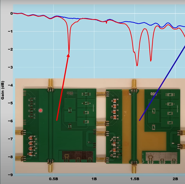
In low‑frequency circuit design, engineers can treat traces simply as connecting wires; as long as the length and width are reasonable, the signal will usually “get there.” However, when frequencies push into the GHz range, the signal’s wavelength shortens to become comparable to the trace length. At this point, every segment of copper foil, every via, and every bend will “reveal” itself in its electrical behaviour.
In practice, common high‑frequency application bands span:
The higher the frequency, the more traces must be treated as controlled‑impedance transmission lines. Otherwise, reflections, radiation, and insertion loss will easily eat up the system’s link budget. In other words, the core of RF PCB design is not “can it connect,” but “can it maintain signal integrity and consistency.”
The substrate material is the first watershed in RF design. The two most discussed physical parameters are the Dielectric Constant (Dk) and the Dissipation Factor (Df).
Dk affects the propagation speed of the signal in the dielectric and directly determines the correspondence between trace width and impedance. If Dk drifts too much with frequency or temperature, it will result in:
For microwave circuits, Dk stability is often more critical than the absolute value of Dk.
Df (also commonly referred to as tan δ) describes the proportion of electromagnetic energy that the dielectric converts into heat. The lower the Df, the less signal attenuation occurs within the substrate. When frequencies exceed 28 GHz, dielectric loss can even surpass conductor loss, becoming the primary contributor to overall insertion loss.
| Material Type | Typical Examples | Target Applications & Characteristics | | :--- | :--- | :--- | | Standard FR‑4 | N/A | Sub‑2.4 GHz applications insensitive to loss (e.g., IoT control boards, peripheral circuits for Bluetooth modules). | | Modified Low‑Loss FR‑4 / Mid‑Tg | N/A | Extends to the 5–10 GHz range; the most cost‑effective compromise. | | Hydrocarbon Ceramic | Rogers RO4350B, RO4835 series | The workhorse for 10–30 GHz. Processability is similar to FR‑4, but with significantly lower Df. | | PTFE (Teflon) Substrates | Rogers RO3003, RT/duroid series | The standard choice for 77 GHz automotive radars and mmWave antennas. great difficulty in lamination and mechanical processing. |
Material selection must balance electrical requirements, process compatibility, and cost. It is crucial to confirm material availability and hybrid lamination needs with the fab house before prototyping.
RF routing is essentially designing controlled‑impedance transmission lines. The three common structures each have their trade‑offs:
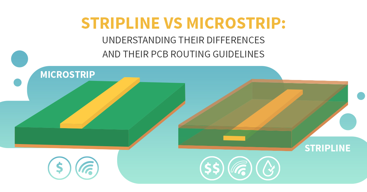 The trace is on the outer layer with a reference ground plane below it.
Grounded copper pours are added on both sides of the microstrip, connected to the underlying ground via dense stitching vias.
The signal layer is sandwiched between two reference ground planes, effectively “burying” the trace within the stackup.
When selecting a structure, comprehensively consider frequency, routing density, isolation requirements, and the fab house’s yield mastery for that specific structure.
In the mmWave bands, a discontinuity of just a few millimetres can ruin your S‑parameters. Key practical principles include:
Many engineers obsess over traces but leave massive electrical discontinuities at the vias. Every via introduces parasitic inductance and capacitance, which significantly impacts return loss at high frequencies.
Practices worth investing effort in:
At microwave frequencies, manufacturing tolerances are directly amplified into electrical performance variations. The following factors all affect impedance and insertion loss:
This is why RF/microwave boards require alignment between the design and manufacturing teams before prototyping. Stackup planning, impedance targets, material selection, and DFM priorities must be clarified upfront, rather than chasing process issues after the prototype fails.
Once the board is fabricated, design assumptions must be verified through actual measurements. Common instruments and measurement items include:
| Instrument | Key Measurements | | :--- | :--- | | Vector Network Analyser (VNA) | S‑parameters (S11 Return Loss, S21 Insertion Loss) | | Spectrum Analyser | Harmonics, spurs, and out‑of‑band noise | | Time‑Domain Reflectometer (TDR) | Locating impedance discontinuity points |
The quality of the calibration kit and the test fixture design often determines the credibility of the measurement results. Especially in the mmWave bands, the fixture’s own impact can sometimes exceed that of the Device Under Test (DUT).
IPC standards frequently referenced in RF and microwave PCB manufacturing include:
While not strictly mandatory, these standards serve as a highly useful common language for acceptance criteria, quality traceability, and cross‑factory collaboration.
The success of an RF and microwave PCB design is never just the result of a layout engineer working alone. It requires:
As wireless systems continue to push toward higher frequencies, smaller sizes, and stricter phase requirements, early collaboration between design and manufacturing will become the deciding factor in whether a product can hit the mark on the first try. The earlier process variables are factored into design considerations, the more predictable and repeatable the RF performance will be during mass production.
