November 20, 2025
To overcome the side etching issues inherent in traditional subtractive processes, semi-additive processes (SAP) and modified semi-additive processes (mSAP) have emerged as the mainstream technologies for IC substrates and substrate-like substrates (SLP). SAP utilizes electrolytic copper as its substrate, delivering the highest circuit precision. mSAP, employing ultra-thin copper foil, strikes a balance between precision and cost, making it a highly cost-effective choice.
mSAP (Modified Semi-Additive Process) and SAP (Semi-Additive Process) are currently critical fine circuit formation technologies in the electronics manufacturing industry, widely used particularly in the production of high-end printed circuit boards (PCBs) and integrated circuit (IC) substrates. These two processes were developed primarily to overcome the limitations of traditional subtractive methods in manufacturing ultra-fine circuits.
| Characteristic Aspect | mSAP (Modified Semi-Additive Process) | SAP (Semi-Additive Process) | |-----------------------|--------------------------------------|-----------------------------| | Core Principle | Selective electroplating to thicken circuits on ultra-thin copper foil (e.g., 2–3 μm), followed by rapid removal of the underlying ultra-thin copper foil via "Flash Etching" | Direct chemical copper deposition on an insulating substrate to form a seed layer, followed by electroplating thickening, and finally etching to form the circuit pattern | | Circuit Precision | Can achieve line width/line spacing below 30 μm / 30 μm (approx. 1.25 mil) | Can achieve finer line width/line spacing below 10 μm | | Process Characteristics | Less undercut, circuit cross-section close to rectangular, more accurate impedance control | Higher circuit precision, but requires stricter overall process conditions and materials | | Cost Considerations | Uses modified substrate materials (like ultra-thin copper foil), considered a cost-effective alternative compared to SAP | Typically requires more expensive special materials, such as ABF (Ajinomoto Build-up Film), resulting in higher overall cost |
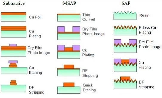
The traditional subtractive method involves covering a thicker copper foil with a resist mask, then removing the unwanted copper via etching. However, this method has significant problems:
Prone to Side Etching
Limited Circuit Precision & Difficult Impedance Control
The principle of both mSAP and SAP is to form conductive traces through an additive approach, rather than etching the circuit pattern out of thick copper foil. The method starts from an extremely thin conductive layer (mSAP) or a seed layer formed by chemical copper deposition (SAP), then uses electroplating to build up copper material where needed.
This approach offers two major advantages:
Significantly Reduces Undercut
Enables Higher Circuit Density
Due to their ability to form fine circuits, mSAP and SAP have become important process technologies in the following high-end areas:
IC Package Substrates
Substrate-Like PCB (SLP, smartphone mainboards)
High-End Servers and Switches
Advanced Packaging like CoWoS, CoWP
When choosing between mSAP and SAP, a balance is typically struck between precision and cost.
SAP
mSAP
From an industry trend perspective, as chip computing power increases, electronic products miniaturize, and high-speed signal demands grow, the requirements for line widths will continue to shrink. The importance of mSAP and SAP will further increase in the future, simultaneously driving technological advancements in key process equipment such as electroplating, etching, and exposure tools.
