May 12, 2026
If you are in the hardware supply chain in 2026, you will undoubtedly feel a harsh reality: the bottleneck restricting the volume production of global AI chips and high-end GPUs lies not only in the advanced nodes of wafer foundries but, more importantly, in the IC substrates beneath the chips and the advanced packaging capacity.
As Moore's Law approaches its physical limits, increasing computing power by scaling down transistors faces a massive cost barrier. Today's industry consensus is centered around "Chiplets" and "Heterogeneous Integration." To clarify this complex technological ecosystem, we must split our perspective into two layers: the evolution of underlying substrate materials and the development of high-density heterogeneous integration architectures. Today, from an engineering practice perspective, we will deeply analyze the underlying logic of the advanced packaging trends in 2026.
The substrate is the physical foundation that carries massive I/O, supplies power, and dissipates heat. For different application scenarios, substrate materials and structures are undergoing significant differentiation.
Despite the constant buzz around new technologies, in the reality of 2026, FCBGA substrates using ABF (Ajinomoto Build‑up Film) materials remain the unshakable mainstream mass‑production solution for high‑end server CPUs and AI accelerators.
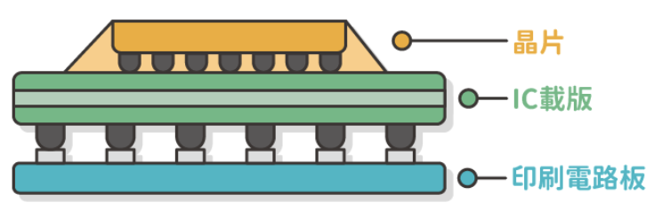
For consumer electronics or specific networking modules, the industry opts to remove the "Core," which provides mechanical support within the substrate.
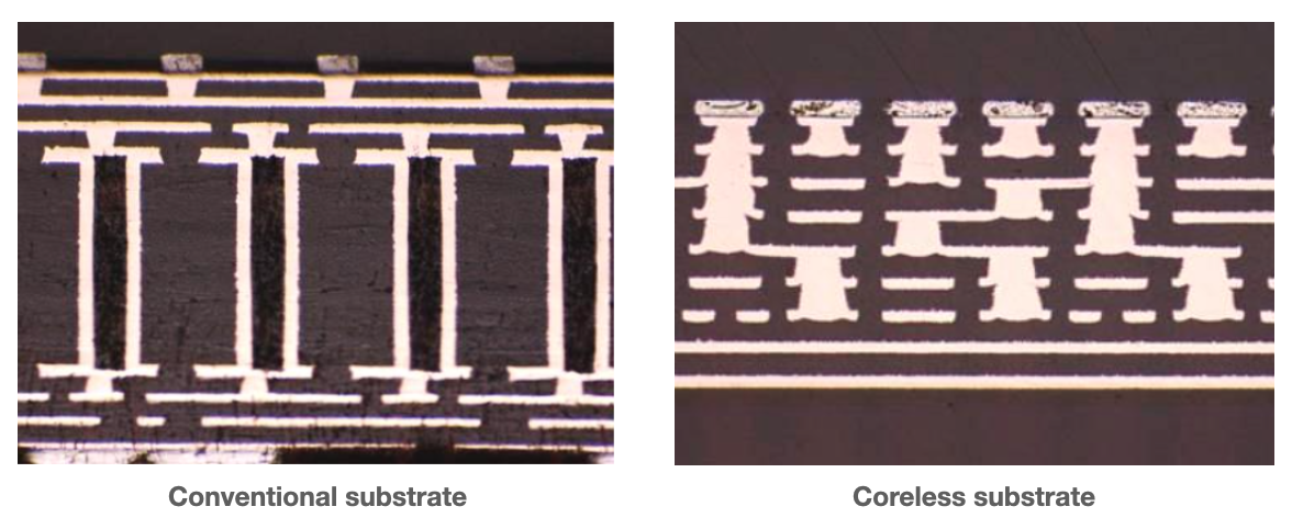
Facing the physical limits of ultra‑large ABF substrates, glass substrates have officially moved from forward‑looking R&D into the engineering validation and early commercialization stages. It is regarded as a vital carrier to extend Moore’s Law, but there is still a long way to go before it fully replaces ABF.
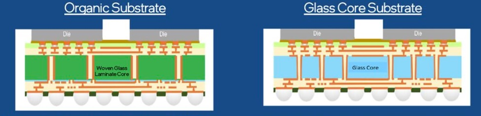
Building upon the foundation of the substrate, how to combine multiple chips from different process nodes in the most efficient and cost‑effective way is the second core issue of advanced packaging.
This is a representative localized bridge solution in current high‑density heterogeneous integration. Instead of using an expensive and area‑constrained full Silicon Interposer, it embeds a small piece of “ultra‑thin silicon bridge” in the localized areas requiring high‑density interconnection. While preserving silicon‑level ultra‑high bandwidth, it drastically lowers manufacturing costs and is widely used in the integration of high‑end GPUs and HBM (High Bandwidth Memory).
To shorten interconnect distances and optimize the Power Delivery Network (PDN), the industry is actively developing embedded technologies.
Advanced packaging and substrates are no longer merely “PCB extensions”; they are highly complex micro‑systems in themselves. In the hardware ecosystem of 2026, the boundaries between system design, chip packaging, and substrate manufacturing have completely overlapped.
For hardware R&D teams, possessing a Co‑Design mindset that spans “Chip Packaging ↔ Substrate ↔ PCB System Board,” and accurately grasping the engineering limits of different substrate materials and the applicable scenarios of packaging architectures, will be the core competitive advantage driving the implementation of next‑generation, high‑performance products.
