May 13, 2026
For hardware RDs and PCB Layout engineers, the term "impedance" is absolutely familiar. But very few can explain it clearly from start to finish. Impedance might seem like just a few simple numbers, but it actually involves complex electromagnetic fields and manufacturing processes behind the scenes. Today, we are skipping the tedious academic theories and using a "Quick Q&A" format to help you sort out the 12 core impedance concepts in DFM practice!
Answer: In a circuit containing resistance, inductance, and capacitance, the obstruction to alternating current is called impedance. It is usually represented by Z, and the unit is the ohm (Ω). It is not a simple addition of resistance, inductive reactance, and capacitive reactance.
In PCB design, impedance refers to the “electrical impedance” between traces, power, loads, and other components on the circuit board. Controlling PCB impedance is the key to ensuring high-speed Signal Integrity. Impedance mismatch will cause signal reflection, which in turn leads to severe noise interference.
Answer: This is a type of characteristic impedance, referring to the impedance of a “single signal trace” relative to a reference plane (GND or VCC) in the circuit. In single‑ended transmission, the signal relies on this single conductor for transmission.

Answer: Used for impedance control of differential signal trace structures. The driver inputs two signal waveforms of opposite polarity, transmitting them simultaneously through two differential traces, and the receiver performs a subtraction process. This method is very common in high‑speed digital and analog circuits and can significantly improve signal integrity and the ability to resist common‑mode noise.
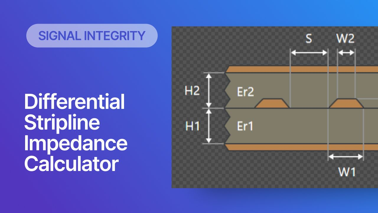
Answer: This is the impedance when a signal trace is accompanied by GND/VCC copper foils on both sides (or one side) during transmission. It is commonly seen in the Coplanar Waveguide (CPW) structure of high‑frequency and microwave circuits. The magnitude of coplanar impedance depends on the conductor trace width, the spacing to the adjacent ground planes, and dielectric parameters.
Answer: 50 ohms has been the industry’s “default standard” for a long time because it strikes an excellent balance between PCB manufacturing convenience and signal attenuation/loss, but this is not an absolute rule. The impedance value depends on the terminal interface; for example, remote communication or video transmission cables often use 75 ohms. Some special chips require lower impedance (e.g., some Intel specifications require control at 42 ohms or even 37 ohms) to improve EMI or crosstalk.
Answer: This is also based on historical evolution and application standards (like early Ethernet). 100 ohms can effectively reduce signal reflection and distortion. Of course, modern high‑speed interfaces have other standards, such as 85 ohms commonly seen in PCIe, and mostly 90 ohms for USB.
Answer: Parallel routing maintains a consistent degree of coupling between the two traces, thereby ensuring impedance continuity along the entire transmission path.
Strictly speaking, as long as the spacing between the two traces is large enough (e.g., > 5 W), the single‑ended impedance of each is properly controlled, and external interference is small, they can transmit without being parallel. But in practice, parallel routing is the safest layout specification with the strongest anti‑interference capability.
Answer: Absolutely not! Length matching is the most critical physical rule for differential traces.
The receiver restores the signal by reading the difference between the two traces. If the lengths are unequal, there will be a phase shift in the arrival time of the signals. In an ideal differential signal, the peak should align with the trough; if the length difference causes a phase shift of 180 degrees, the signals will completely cancel each other out and cause an error. Even a phase shift of just 30 degrees will severely squeeze the margin of the eye diagram and convert the differential‑mode signal into common‑mode noise. Generally, the specification error must not exceed 5 mils, with an absolute limit of 10 mils.
Answer: Theoretically yes. This is called Broadside Coupling, which is very useful for escaping high‑density BGAs and can cancel out the Fiber Weave Effect of PCB materials.
However, it is strongly discouraged in DFM practice. Because PCB lamination will inevitably produce interlayer registration errors, which will cause the top and bottom traces to fail to overlap perfectly, resulting in drastic impedance changes and extremely high manufacturing risks. This type of routing is especially a major taboo in HDI (High‑Density Interconnect) boards.
Answer:
Answer:
Answer: The most standard and authoritative simulation tool in the industry is absolutely Polar Instruments (such as Si9000). During stack‑up design and DFM review, Polar can accurately simulate the changes in single‑ended, differential, and coplanar impedance based on the actual material parameters (Dk/Df, resin content, etc.) provided by the board manufacturer. It also supports reverse calculation functions (inputting target impedance to find trace width/spacing), making it a must‑have tool to ensure zero impedance errors before releasing the PCB for production.
