May 13, 2026
As Wi-Fi 7 (IEEE 802.11be) officially transitions from early technology demonstrations to mass production deployments in both enterprise and consumer markets, the industry's focus is often fixated on its theoretical transmission speeds of up to 40 Gbps and ultra-low latency. However, stepping back to the hardware foundation, Wi-Fi 7 is by no means as simple as just swapping out a main control chip. From the massive 320 MHz channel bandwidth to Multi-Link Operation (MLO), these protocol leaps are imposing severe physical challenges on the underlying substrates and printed circuit boards (PCBs). For the Taiwanese supply chain, which has long dominated global networking equipment OEM and PCB manufacturing, this 2026 replacement wave is both an opportunity for capacity expansion and a watershed moment for high-end manufacturing capabilities.
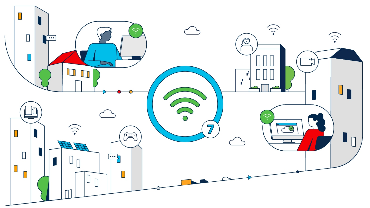
One of the most disruptive technologies in Wi‑Fi 7 is Multi‑Link Operation (MLO). Past devices could only connect to either 2.4 GHz, 5 GHz, or 6 GHz. MLO allows devices to transmit and receive data across multiple bands simultaneously. This means that within the confined space of an enterprise Access Point (AP), multiple Radio Frequency Front‑End Modules (FEMs) must operate at full speed concurrently.

As the number of antennas increases (high‑end APs even support 16 spatial streams) and various IoT Bluetooth/UWB modules are integrated, the layout space on networking motherboards is severely compressed.
High‑end HDI (High‑Density Interconnect) processes, previously rare in general low‑to‑mid‑range networking products, are gradually becoming standard configurations in the Wi‑Fi 7 era. We are seeing a shift from the common 2+N+2 to 3+N+3, and even moving towards Any‑Layer HDI. Blind and buried via designs are not just for saving space; they are primarily used to shorten via lengths, reduce parasitic capacitance, and minimise residual stub effects, thereby ensuring high‑frequency signal integrity.
Performance enhancements are accompanied by soaring power consumption. Modern Wi‑Fi 7 APs feature dual 10 Gbps Ethernet interfaces and integrate edge computing capabilities. Traditional 30 W PoE (Power over Ethernet) is no longer sufficient, making comprehensive upgrades to 802.3bt (60 W or even higher) the norm.
This brings severe thermal management issues to the PCB. The main control SoC and RF modules generate immense heat within the confined, enclosed AP casing. Therefore, during the DFM (Design for Manufacturability) stage, we are seeing an increasing number of designs incorporating Heavy Copper processes (such as 2 oz or 3 oz inner layer copper foil) to assist in high‑current transmission and heat conduction. Some designs even employ embedded Copper Coin technology beneath critical heat‑generating components. Balancing high‑frequency fine lines while handling the resin filling difficulties and warpage risks associated with heavy copper lamination is currently the most critical process pain point that factories must overcome.
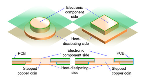
As a global R&D and manufacturing hub for enterprise networking equipment (such as switches, routers, and enterprise APs), Taiwan is at the epicentre of this wave of technological transition.
In the 2026 Taiwan market, simply “building to print” can no longer meet the expectations of major North American networking giants. Faced with Wi‑Fi 7’s complex stack‑ups, extreme high‑frequency material properties, and rigorous thermal demands, PCB manufacturers must intervene much earlier in the hardware R&D cycle. By utilising front‑end DFM checks, Polar impedance simulations, and material library matching, manufacturing risks must be eliminated right at the layout stage.
Wi‑Fi 7 undoubtedly brings an ultimate wireless experience, but it is not magic; it is built on extremely precise physical engineering. For the PCB industry, this is not merely a material upgrade, but a comprehensive stress test covering signal integrity, high‑density routing, and thermodynamic management. Only those suppliers who master these underlying manufacturing know‑hows will possess the absolute advantage to secure enterprise client orders in the networking replacement wave over the next three years.
