I. The Core Value of Heavy Copper PCBs: Not Just Conduction, But Structural Support
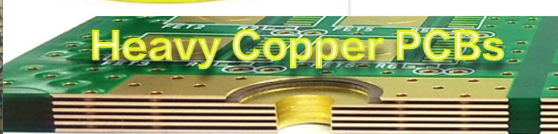 The core advantage of heavy copper PCBs lies in their extremely low direct current resistance (DCR) and outstanding thermal conductivity. Taking automotive power modules as an example, when the system needs to continuously withstand large currents, ordinary thin copper boards will quickly heat up due to the Joule heating effect, leading to substrate aging or even burning. Heavy copper not only efficiently channels the current but also acts as a heat dissipation path, quickly guiding heat to the metal casing or heat sink fins.
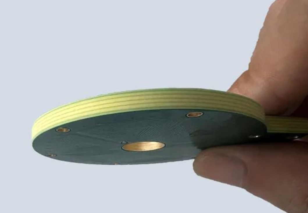
Furthermore, heavy copper stack-ups significantly enhance the mechanical strength of the PCB. The thick copper layers act like rebar added to the circuit board, greatly improving its bending resistance and vibration resistance, which is crucial for harsh industrial or automotive-grade vibration environments.
II. The Golden Rules of Routing and Stack‑up: Precise Balance of Performance and DFM
1. The Science of Copper Thickness Selection: Farewell to the “Thicker is Better” Myth
The primary principle of heavy copper design is “precise matching based on current carrying capacity.” Blindly increasing copper thickness not only causes manufacturing costs to soar but also triggers severe lamination resin starvation and poor etching issues.
- Current Carrying Evaluation Reference: It is recommended that Layout engineers directly refer to the IPC‑2152 standard for temperature rise and trace width calculations. As a general rule of thumb, a 3 oz copper foil paired with a 3 mm trace width can carry approximately 7 A‑8 A of current at a 40 °C temperature rise.
- Selection Suggestions: For most industrial and power supply applications, 3 oz to 8 oz is the “sweet spot” with the highest cost‑effectiveness and relatively mature processes. Unless there is an extreme requirement, avoid using ultra‑heavy copper across the entire board. Consider localized heavy copper (embedded copper processes) or concentrated optimisation on critical high‑current paths, while maintaining 1 oz‑2 oz in non‑high‑current areas.
2. Routing Design: Reserving Undercut Compensation and Smooth Transitions
Heavy copper etching is fundamentally different from thin copper. The thicker the copper, the more severe the “undercut” phenomenon – where the etchant bites laterally while etching vertically downward – resulting in a trapezoidal trace cross‑section.
- Line Width / Space (L/S) Limits:
- 3 oz Copper Foil: Minimum trace width/space is recommended to be ≥ 8 mil / 8 mil (approx. 0.2 mm).
- 6 oz – 8 oz Copper Foil: To ensure etching yield, the trace width/space must be relaxed to ≥ 15 mil / 15 mil (approx. 0.4 mm) or more.
- Smooth Transition Design: High‑current paths must avoid 90‑degree right angles or sudden changes in trace width. Gradual transitions (tapering) or large‑area teardrops must be used, with a transition length recommended to be ≥ 3 times the width difference, to eliminate “current bottlenecks” and localised hot spots.
- Large Area Copper Pour: Large areas of solid copper pour are highly prone to board warping due to thermal stress when passing through the SMT reflow oven. It is recommended to use hatched copper pours. If solid copper pours must be used, thermal and stress relief slots must be reserved.
3. Via Design: Opening the Z‑axis Thermal and Electrical Channels
- Hole Diameter and Copper Wall: Heavy copper boards are usually thicker, requiring attention to the aspect ratio of mechanical drilling. The minimum hole diameter is recommended to be ≥ 0.8 mm, and the board manufacturer should be required to plate the hole wall copper thickness to at least 20 μm – 25 μm or more.
- Via Arrays (Stitching): When facing tens of amperes of current, you absolutely cannot rely on a single via. When high‑current paths change layers, via arrays must be utilised. Estimate the single via carrying capacity at 2‑3 A, and connect multiple vias in parallel to divert the current and reduce parasitic inductance and resistance.
- Solder Mask Opening: Sufficient solder mask openings (0.1‑0.15 mm larger than the hole diameter per side) must be reserved around heat dissipation and high‑current vias to prevent the green mask from entering the hole, which could cause bubbling or board bursting risks during subsequent assembly.
III. Key DFM Considerations on the Manufacturing Side
As a hardware designer, understanding the factory’s limits in advance can save the company countless rework costs due to assembly failures.
1. Lamination Process and Resin Flow Control
When inner layer traces reach 4 oz or even 8 oz, the “deep trenches” between traces require a large amount of resin to fill.
- High Resin Content Prepreg (PP): Board manufacturers must use high‑resin‑content PP (such as 1080 or even special high‑resin specifications); otherwise, micro‑voids will easily form at the edges of the traces, triggering subsequent Conductive Anodic Filament (CAF) short‑circuit failures.
- Stack‑up Symmetry: Regardless of the number of layers or copper thickness distribution, the principle of Z‑axis symmetry must be strictly observed. If the Top layer is 6 oz and the Bottom layer is 1 oz, the probability of board warpage after high‑temperature lamination and SMT is extremely high.
2. Substrate (CCL) and Solder Mask Selection
- High Tg Materials: Heavy copper boards absorb a massive amount of heat during the SMT stage and dissipate it slowly. It is strongly recommended to use mid‑to‑high‑end FR‑4 with Tg ≥ 170 °C (such as common High Tg CCLs) to ensure that Z‑axis thermal expansion (Z‑CTE) is controlled under prolonged high‑temperature reflow soldering, protecting the hole copper from being torn apart.
- Solder Mask Coverage: Due to the large height difference of heavy copper traces, the solder mask at the corners of the traces is often the thinnest, making edge copper exposure highly likely during wave soldering. During layout, notes should be added to the Gerber files requiring the board manufacturer to perform double solder mask printing to ensure sufficient thickness.
3. SMT Assembly Adaptation
- Thermal Relief Pads: If high‑power components (such as TO‑220, D²PAK) are directly connected to large areas of heavy copper, overly rapid heat dissipation will lead to cold solder joints or false welding. Standard thermal relief pads (spoke connections) must be designed to balance the thermal capacity during soldering.
- Stencil and Oven Temperature: The assembly plant needs to appropriately increase the peak temperature of reflow soldering for heavy copper boards (by about 5‑10 °C) and extend the soaking zone time to ensure the solder paste melts completely.
IV. Summary
Excellent heavy copper PCB design is definitely not just about drawing thicker lines in EDA software. It is a mutual convergence of “current channel design” and “factory process limits.” By mastering the three core aspects of precisely evaluating copper thickness, optimising tapering and via arrays, and proactively considering the DFM boundaries of lamination and etching, you can get your high‑power design right the first time and safely pass various rigorous reliability tests.
