May 31, 2026
In the era of explosive AI computing power, high-speed servers demand exceptional Signal Integrity (SI). Signal transmission loss in high-speed PCBs is primarily divided into dielectric loss (related to the material's dielectric constant Dk and dissipation factor Df) and conductor loss (caused by the high-frequency skin effect and copper foil surface roughness). To minimize loss, strictly selecting low-loss materials and refining the circuitry process are essential. However, depth-controlled drilling technology (commonly known as backdrilling) is the ultimate key. Backdrilling effectively removes redundant via stubs, eliminating signal reflection and scattering, minimizing signal distortion, and ensuring the stability of high-speed transmission. This article uses a 22-layer server motherboard as a case study to deeply explore the pain points of its mass production process and viable solutions.
The 22‑layer server motherboard developed for this project has a finished board thickness of 2.95 mm ± 10%. The inner layers consist of 1/1 oz and 2/2 oz core boards, with a design trace width of 3.5 mil and an aspect ratio reaching 14.75:1. It also utilises a Plated Over Filled Via (POFV) process.
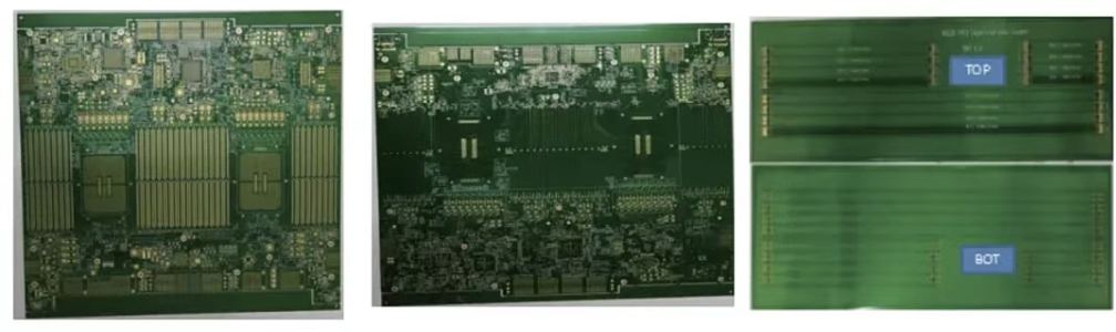 Trial Anomaly: After manufacturing through the traditional workflow, the insertion loss significantly exceeded the standard, and the hole copper thickness was excessively thick, failing to meet the strict SI standards.
The process engineering team established a four‑factor, two‑level full factorial Design of Experiments (DOE). The key variables investigated were: trace width compensation, prepreg (PP) resin content, panel rotation angle, and brown oxide micro‑etching solution.
By measuring the loss values of the 85‑ohm transmission line at various high frequencies, the optimal process parameters (Scheme 11) were identified:
| Experimental Condition Combination (Optimal) | 4 GHz Inner Layer Measured Loss | Specification Upper Limit | Comprehensive Assessment | | :--- | :--- | :--- | :--- | | +0.2 mil width compensation + 75% high‑resin PP + ultra‑low roughness solution + 7‑degree panel tilt | 0.286 dB/inch | 0.350 dB/inch | Significantly passed; lowest loss achieved |
The conventional process requires three plating cycles (Panel Plating, Capping Plating, Pattern Plating), resulting in backdrilled holes with excessively thick copper and undersized diameters. The team reorganised and optimised the conventional process:
Original Flow (Traditional)
Material Cutting → Inner Layer → Lamination → Laser Blind Via → Drilling 1 (Through‑holes + depth‑control drilled at once) → Panel Plating → Pattern Plating 1 → Resin Plugging → Copper Grinding/Reduction → Capping Plating → Outer Layer → Pattern Plating 2 → Backdrilling → Etching.
New Flow (Flipped Optimisation)
Material Cutting → Inner Layer → Lamination → Laser Blind Via → Drilling 1 (Only vias requiring plugging) → Panel Plating 1 → Pattern Plating 1 → Resin Plugging → Copper Grinding/Reduction → Drilling 3 (Remaining non‑plugged through‑holes) → Panel Plating 2 → Outer Layer → Pattern Plating 2 → Final Backdrilling → Etching.
Improvement Benefits: The drilling process was decoupled into a two‑stage operation. The plugged holes and Capping plating were handled first, and standard signal through‑holes were drilled in the second stage. This successfully prevented all backdrilled holes from undergoing three repetitive copper platings, completely resolving the pain points of copper over‑thickness and backdrill diameter shrinkage.
Material Cutting & Inner Layer
After cutting, a 190 ℃ × 4 hour mandatory bake is performed to release stress. Inner layers utilise high‑precision LDI exposure, with trace width/spacing at 3.5 / 4.0 mil, and impedance trace width tolerance strictly controlled within ±8%. The AOI fine‑line inspection function is enabled, and trace patching is strictly prohibited.
High‑End Lamination
Seven registration pins are used to closely monitor layer shift. A low‑roughness brown oxide line is selected. Lamination uses a dedicated high‑end profile with the vacuum extraction time extended by 5 minutes to ensure 100% saturated resin filling. Dielectric thickness tolerance is controlled within ±10%.
First‑Stage Drilling & Plating
Drill 1 only targets holes requiring resin plugging. Drill bits for hole diameters < 0.5 mm are set for mandatory replacement after 500 hits (CPK > 1.33). After Plasma desmear, the boards enter a pulse plating line to ensure initial hole copper reaches 0.9 – 1.0 mil.
Resin Plugging & Copper Grinding
San‑Ei 10HF resin from Japan is used for double‑sided plugging, achieving 100% fullness. Grinding maintains surface copper at 1.2 – 1.5 mil, followed by a dedicated micro‑etching line to evenly reduce base surface copper to 0.9 ± 0.1 mil.
Second‑Stage Drilling & Final Pattern Plating
A CCD drill machine creates the remaining standard through‑holes (hole position tolerance ±0.05 mm). The second round of panel and pattern plating is performed. Final finished requirements: surface copper Min 1.9 mil, hole copper Min 0.8 mil, and Capping plating dimple over plugged holes < 25 µm.
Post‑Process Control
Final backdrilling is executed (Stub strictly controlled at 7 ± 5 mil), followed by a 2.5 kg/cm² high‑pressure wash. Electroless Nickel Immersion Gold (ENIG) requires a gold thickness of 2 – 10 µ" / nickel thickness Min 118 µ", with nickel corrosion strictly controlled at < 20% to prevent black pad defects.
Through integrated process optimisation in this project, all SI performance indicators were perfectly met:
Impedance Control: The 85 Ω and 100 Ω transmission lines on inner layers yielded measured values between 83.8 – 102.5 Ω, all passing inspection.
Insertion Loss (Delta‑L test method, 10‑inch transmission line) :
| Testing Frequency (GHz) | Inner Layer Measured Loss (dB/inch) | Outer Layer Measured Loss (dB/inch) | Industry Standard Upper Limit (dB/inch) | SI Comprehensive Assessment | | :--- | :--- | :--- | :--- | :--- | | 4.0 GHz | 0.286 | 0.312 | 0.350 | Passed (Excellent) | | 8.0 GHz | 0.495 | 0.534 | 0.600 | Passed (Excellent) | | 12.89 GHz | 0.721 | 0.785 | 0.850 | Passed (Excellent) | | 16.0 GHz | 0.884 | 0.942 | 1.050 | Passed (Excellent) |
The overall FPY for the initial release of the high‑layer‑count (>10L) trial boards reached over 85%:
Prepreg Stack‑up Optimisation
High‑speed signal layers should prioritise prepregs with a high resin content (RC 75%), which can further reduce high‑frequency transmission loss by an additional 1% – 3%.
Specify Low‑Roughness Chemical Processes
Comprehensively introducing ultra‑low roughness brown oxide chemistry to replace traditional black/brown oxide can directly optimise insertion loss by 3% – 7%.
Layout Rotation Routing at 7 Degrees
Setting a 7‑degree angle between the layout routing direction and the glass fibre bundle direction (anti‑fibre weave effect) can reduce high‑frequency loss by an additional 2% – 3% compared to the traditional 3‑degree layout.
Implement a Two‑Stage Process Flow
For deep‑hole, thick boards with POFV and high‑frequency backdrilling requirements, decoupling the drilling into a “two‑stage drilling and plating” flow is the optimal manufacturing path to balance surface copper flatness and a high SI pass rate.
