June 1, 2026
Recently, the hottest keyword in TSMC's supply chain has shifted from CoWoS to CoPoS—a one-letter difference that could rewrite the rules of advanced packaging. The W in CoWoS stands for Wafer, the familiar round silicon disc; the P in CoPoS stands for Panel, a square or rectangular panel. TSMC Chairman C.C. Wei proactively confirmed the progress of this technology for the first time during the April 2026 earnings call, sending related concept stocks surging. The question is: Why replace a perfectly good wafer with a panel? This article dives into the often-overlooked reality that "the wafers we are familiar with are simply no longer enough." We will explore the formidable physics "bosses" behind this circle-to-square transition that can drop yields to zero, and how industry giants are defeating them one by one.
We often hear Moore's Law dictates that chips will get smaller. That's only half true—it makes the transistors inside the chip smaller, yes. However, with the explosive demand for computing power from AI and large language models (LLMs), we want to pack so much into them that the overall area of a single chip is actually getting larger.
Not to mention the current trend of combining a massive GPU with an entire row of High Bandwidth Memory (HBM), piecing them together like a puzzle into a colossal chip module. The larger the chip, the fewer complete chips can be cut from a circular wafer, leading to more severe edge waste.
So why not just make the wafer bigger, like a massive 20‑inch pizza? The answer lies in the material itself.

A wafer isn't a rock picked up off the street; it requires a strict single‑crystal silicon structure with a purity of up to 99.999999999% (the legendary "eleven nines").
Manufacturing this perfect material is almost like alchemy. Scientists use a technique called the Czochralski process. They heat purified liquid silicon to over 1414 °C, drop in a tiny, perfect silicon crystal as a "seed," and pull it upwards extremely slowly while rotating it. The liquid silicon gradually solidifies following the atomic arrangement of the seed crystal, ultimately forming a giant, flawless cylinder—a silicon ingot.
Herein lies the problem: monocrystalline silicon requires a 100% perfect atomic arrangement. If even a single atom is out of place, creating a crystal lattice defect, the current will run amok, and the wafer is instantly scrapped.
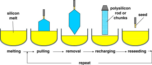 And when you greedily try to increase the diameter of the silicon ingot (e.g., pulling it to 18 inches), you hit an impassable wall: temperature difference.
Imagine putting a large bucket of water in the freezer: the outer ring freezes solid while the centre remains a high‑temperature liquid. This push‑and‑pull of internal and external thermal expansion and contraction (thermal stress) will directly tear apart the perfectly arranged atoms, creating massive dislocations.
In other words, even if you get incredibly lucky and pull an 18‑inch‑thick silicon ingot, slicing it open will reveal defective products full of misaligned atoms, completely useless for high‑end chips. This is why wafer sizes are strictly capped by physical limits and cannot grow any larger.
If you can't make circles bigger, how about squares? The industry happens to have a technology called Fan‑Out Panel‑Level Packaging (FOPLP): it abandons the traditional circular wafer entirely and instead places chips on a large square carrier board.
Square panels offer two overwhelming advantages:
How direct is the impact? Take the NVIDIA B200 as an example: a 12‑inch circular wafer can only package 4 sets. Switching to a square panel of the same size allows for an estimated 9 to 16 sets conservatively—effectively "invisibly expanding" production capacity by more than double under the same material footprint.
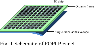
To understand CoPoS, we must first review CoWoS. Because AI chips and memory require highly dense, ultra‑high‑speed data transmission, all top‑tier AI chips today use CoWoS (Chip‑on‑Wafer‑on‑Substrate) packaging.
Think of it as a luxury residential community: bare dies aren't built directly on a regular circuit board; instead, they sit snugly together on an expensive silicon interposer. This silicon interposer is packed with microscopic interconnect channels, like underground high‑speed rails, allowing chips to frantically exchange data with ultra‑low latency. It's fast and stable, but the downside is that it is extremely expensive and time‑consuming.
The fatal bottleneck is this: the raw material for the silicon interposer is, ultimately, a circular wafer sliced from a cylindrical silicon ingot. As the area of the interposer grows, so do the square odd‑shaped wastes on the circular wafer.
To break this bottleneck, engineers must abandon the familiar silicon substrate and switch to large panels with glass or organic materials at their core—this is CoPoS.
Therefore, CoPoS is not just an extension of FOPLP. Its true identity is a hybrid technology born after CoWoS hit the physical bottleneck of area while pursuing ultimate performance, turning to borrow FOPLP's "squaring the circle" experience, and completely overhauling the underlying materials. In industry terms, CoPoS is seen as the next‑generation version of CoWoS, but the difference between the two is far more than just "Wafer turning into Panel."
Changing materials sounds great, but disaster quickly follows.
Different materials expand at vastly different rates when heated—silicon expands little, copper wire a bit more, and the organic encapsulant holding the chips expands several times more than silicon. The packaging process involves enduring high temperatures over 200 °C before cooling down. Materials with a high Coefficient of Thermal Expansion (CTE) shrink aggressively, while those with a low CTE stay firmly in place.
Imagine tightly gluing a highly elastic rubber band to a hard wooden board, tossing it in the oven, and taking it out: the rubber band shrinks wildly, the wood doesn't, and the whole board is pulled into a severe curve. The larger the panel area, the more exaggerated this warpage becomes, making subsequent processes simply impossible.
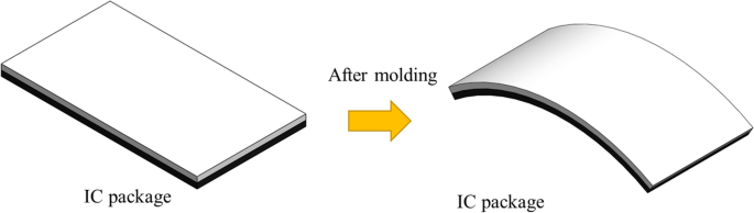
The machine first attaches thousands of expensive chips onto a carrier with nanoscale precision, then injects liquid encapsulant, heating it to cure. The problem lies in curing shrinkage—when polymer colloids transition from liquid to solid, molecular chains link and pull closer together, causing an irreversible shrinkage in overall volume that violently drags the originally precisely aligned chips out of place.
On a large panel, this shift is continuously amplified. Even a deviation of just 2–3 µm means that in the subsequent circuit‑drawing process, the microcircuits won't align with the chip contacts. Unaligned contacts mean an open circuit, instantly dropping the yield of the entire expensive AI chip to zero.
Since organic materials shrink chaotically upon heating, the solution is to switch to a material that doesn't. The tech giants' answer: replace the substrate core with glass.
Glass has formidable advantages:
How is it adjusted? There is some very elegant material chemistry at play here:
By tuning the scaling of glass in this way, the massive warpage caused by pulling from both sides is fundamentally eliminated.
But glass's biggest nightmare is its brittleness. To connect circuits layer by layer, tens of thousands of Through‑Glass Vias (TGVs) must be drilled and filled with copper. Remember the thermal expansion boss? Copper expands with immense force when heated; as it expands inside the via, it can directly crack the fragile glass from the inside out.
The solution is to plate an elastic buffer layer at the interface between the copper pillar and the glass, usually made of polyimide. It is highly elastic at a microscopic level, essentially padding a layer of "drop‑proof sponge" before filling the copper. When the copper expands, the sponge absorbs the stress, allowing the glass substrate to survive thousands of extreme hot‑and‑cold shocks.
Warpage is solved, but what about the chip shift caused by encapsulant shrinkage? Engineers deploy a continuous "hard and soft" combo.
Traditional encapsulants were either too soft to hold the chips or too hard and prone to cracking. Japanese material giants developed a new type of encapsulant compound by adding special flake‑like fillers to the formula. This gives the cured glue immense mechanical hardness (resistance to indentation, scratching, and permanent deformation), locking the chips down as if growing muscles to prevent them from running amok due to shrinkage stress.
Even with the strongest glue, chips on a large panel might still shift a few micrometres. Traditional optical lithography machines use physical photomasks to project circuit patterns—like stamping an image or hanging wallpaper. If the seam between two complex wallpaper patterns is even slightly off, the pattern breaks (academically known as a stitching error). If the chip underneath is crooked, the rigid stamp coming down on top will definitely miss the mark.
Optical giant Nikon's disruptive, innovative machine completely scraps the physical photomask, switching to digital projection: when sensors detect that the bottom‑layer chips on the panel have shifted, the computer instantly recalculates and intentionally distorts and morphs the projected digital circuit pattern. If the chip skews to the left, the circuit pattern skews to the left along with it, perfectly matching the coordinates of every shifted chip. Through this digital tolerance of "you warp, I warp with you," the risk of disconnected wires is eliminated, forcibly rescuing the yield.
Looking at the entire industry transition period, the biggest bottleneck to mass production has long ceased to be equipment or basic material R&D; it is stuck on yield.
The reasoning is painfully realistic: a giant panel houses next‑generation AI logic chips, flanked by a luxurious array of HBM4 memory. A drop in yield of just a few percent results in astronomical financial losses. The larger the panel size, the higher the difficulty of process control, which was one of the main reasons CoPoS mass production schedules were once delayed.
In terms of timeline, the current clearer version is:
On the supply chain side, aside from major European, American, and Japanese companies like KLA, TEL, Applied Materials, and Disco, 13 Taiwanese manufacturers have also made the initial supplier list, covering wet processes, automated equipment, and packaging and testing.
It is worth noting that even though C.C. Wei actively mentioned CoPoS during the April earnings call, he still emphasised that AI demand far outstrips supply, and TSMC is working hard to provide sufficient capacity at a reasonable cost. In other words, CoWoS is currently still playing catch‑up on capacity; CoPoS is an early layout for the "larger, greedier next generation of AI chips."
For R&D professionals in Taiwan, the value of the CoPoS topic lies not just in news headlines like "TSMC takes the lead again," but in its demonstration of a hard engineering truth:
When you hit a physical limit in a certain dimension (the circular silicon wafer), rather than stubbornly pushing material purity, it is better to change the geometry and material system to solve the problem anew.
Behind "squaring the circle," CTE matching, copper expansion in glass vias, and digital exposure to compensate for chip shift are all classic examples of "cross‑material, cross‑process" collaborative design. This kind of thinking can be applied to any team working on packaging or heterogeneous integration.
Going forward, there is only one real metric to keep an eye on: whether the yield can climb to an acceptable level before mass production in 2028.
