March 4, 2026
Poorly manufactured edge semi-plated holes are not merely an aesthetic issue—they are a nightmare of skyrocketing rework rates and batch short circuits. Many R&D teams only realize the problem when their boards are rejected by the assembly factory. They then discover that the cutting stress generated by clockwise rotating CNC milling cutters directly causes copper skin delamination at the “B point” of the semi-plated hole. In today's pursuit of modularity and extreme space utilization, edge castellated holes have become the core technology for board-to-board connections. But if you don't understand forming stress management, this board will be a shredder for your wallet.
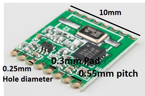
The manufacturing logic of edge castellated holes is to first drill completely plated through holes (PTH), and finally use a CNC router bit or laser to "cut the holes in half" during the profiling stage.
In PCB manufacturing, the router spindle defaults to clockwise rotation. When the tool cuts into the plated hole, two areas with completely opposite forces are generated:
⚠️ Note: If these residual copper burrs fall between SMT pads, they can cause micro-shorts in minor cases, or lead to complete communication failure in an RF module in severe cases.
A successful castellated hole board depends half on the board manufacturer and half on decisions made during your Layout phase.
| Parameter Item | Recommended Minimum (Standard) | Advanced Limit (Advanced) | Key Purpose | | :--- | :--- | :--- | :--- | | Finished Hole Size | ≥ 0.6 mm | 0.4 mm | Ensure plating solution circulation and in-hole copper thickness | | Hole Pitch | ≥ 1.0 mm | 0.8 mm | Prevent solder bridging and profiling stress interference | | Minimum Annular Ring | 0.25 mm | 0.18 mm | Provide sufficient adhesion area to prevent peeling | | Pad to Board Edge Distance | ≥ 1.0 mm | 0.5 mm | Increase the anchoring strength of copper foil to the substrate |
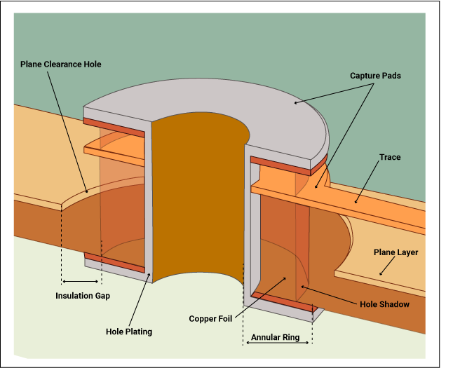
This is a pit-avoidance secret among senior RDs: add "Inner Layer Pads" at the castellated hole locations.
These inner copper foils combine with the vertical copper tube of the hole wall to form a structure similar to a "rivet," firmly nailing the plated copper layer into the substrate. This can significantly counteract the horizontal shear force at Point B and is the most effective design method to reduce copper lifting.
If your project has extremely high requirements for edge flatness (e.g., for aerospace or high-speed communication modules), please confirm that your supplier has the following two processes.
For high-precision products, the standard process will be adjusted to:
After cutting is complete, alkaline etching or chemical micro-etching is used to precisely remove any remaining fine copper wires. This technology can achieve near-perfect edge quality, meeting IPC-A-600 grade requirements.
The surface finish of castellated holes directly determines the assembly yield.
When designing castellated holes, you must simultaneously consider the "Aspect Ratio (AR)." This is the most realistic boundary determining your PCB quotes.
The aspect ratio calculation formula is: AR = Board Thickness / Drill Hole Diameter. When AR > 10:1, it is extremely difficult for the plating solution to circulate within narrow and deep holes, resulting in insufficient copper thickness in the center of the hole.
When your design requires a hole diameter of less than 0.2 mm and the AR soars, you should decisively switch to 1-stage or 2-stage HDI. By using lasers to drill Microvias, although the unit price per board is higher, it can effectively shorten the signal path and save routing space. Ultimately, the Total System Cost might actually be lower.

In Taiwan's rapid PCB prototyping market, eCloud PCB is dedicated to solving the pain points of highly difficult drilling and castellated hole processing.
We have introduced advanced Pulse Plating technology, ensuring that in thick server board designs with an AR exceeding 12:1, the copper thickness in the center of the hole still meets the IPC Class 3 requirement of 25 μm or more, eliminating deep-hole reliability failures from the root.
Furthermore, our platform supports 24H urgent orders and automated DFM checks, helping RDs identify insufficient anchoring or spatial conflict issues in castellated hole designs at the very first opportunity.
In today's increasingly competitive electronics market, "tiny details determine the success or failure of mass production." Only by understanding the underlying logic of stress and cost in castellated boards can you defend your company's profit sweet spot on the design blueprint.
If you are working on a next-generation modular design, feel free to consult the eCloud DFM team. We will accompany you in conquering the final mile of hardware development.
