March 4, 2026
Today, as 3 oz, 4 oz, and even 6 oz thick copper boards become standard for AI servers and high-power power supplies, many RD engineers hold an intuitive belief: “Thicker copper means better heat dissipation and safer current carrying.” However, in nodes exceeding 20A or 50A, the components that actually burn out and cause catastrophic failures are rarely the main traces. Instead, it's the connecting ribs of the thermal relief pads. While viewed as a DFM compensation tool to address assembly yield during design, these ribs can become lethal “invisible fuses” during mass production and operation. This article dissects the true engineering red lines of thick copper board design—from physical mechanisms and IPC-2152 derating guidelines to the process limits of 12:1 deep-hole plating.
Compared to the standard 1 oz copper weight, heavy copper technology can significantly increase the cross-sectional area of the conductor. When current increases exponentially, the heat generated increases quadratically. Increasing copper thickness is the most direct way to suppress temperature rise. During operation, a heavy copper layer acts like a large onboard heat sink, rapidly spreading heat from hotspots.
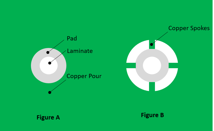 However, this excellent thermal conductivity becomes a nightmare during "assembly."
When an automated assembly line tries to heat a pad to melt solder paste, the large copper plane acts like a "thermal sponge," instantly wicking away the heat. This prevents the pad from reaching the liquidus temperature, resulting in severe cold solder joints or tombstoning effects. To artificially create a "thermal bottleneck" and retain heat on the pad, the Thermal Relief pad was developed.
🔴 Engineering Red Line Summary:
The most dangerous mistake in heavy copper design is neglecting the "current crowding" phenomenon on the connecting spokes.
During normal operation, the slender connecting spokes of a thermal relief pad are the narrowest bottleneck in the entire current path. When high current passes through, the localized temperature rise further increases the resistance of the copper, generating more heat and creating a vicious cycle. If the designed cross-sectional area is insufficient to handle the inrush surge current, the spokes can vaporize and fuse instantly, just like a fuse.
According to the IPC-2152 standard, inner layers dissipate heat more slowly, so the conductor width requirements for their thermal relief spokes are typically 50% to 70% higher than for outer layers.
Safety Reference Values for 3 oz Copper, 4-Spoke Configuration:
| Load Current | Target Temp. Rise | Minimum Width per Spoke | Failure Risk Analysis | | :--- | :--- | :--- | :--- | | 5A | 10°C | 0.25 mm | Low risk, excellent manufacturing safety | | 10A | 10°C | 0.55 mm | Need to account for line width reduction due to etching tolerances | | 20A | 20°C | 1.20 mm | Borderline, risk of cold solder joints | | 50A+ | 30°C | Recommend Avoiding | Extremely poor, high risk of direct fusing |
🔴 Engineering Red Line Summary:
Design isn't about blindly applying rules, but knowing when to break them. In cases of extreme high current, to ensure operational safety, you must decisively abandon thermal relief pads and adopt active process compensation instead.
Switch to a Solid Connection in the following situations:
Supporting Process Compensation Strategy: Abandoning thermal relief means assembly difficulty increases sharply. In the design specification, explicitly require the assembly house to use techniques like hot plate preheating (preheating the PCB above 100°C) or nitrogen reflow. This uses process assistance to share the thermal burden created by the design choice.
Having addressed planar current issues, the next challenge is vertical interconnection. For R&D engineers, design isn't just about electrical performance; it's also about the product's cost structure. PCB drilling is where cost fluctuates most dramatically.
Aspect Ratio (AR = Board Thickness / Hole Diameter) is key to determining plating quality and cost. The higher the AR, the harder it is for plating solution to enter deep holes, making Plating Voids (no copper in the hole center) likely, which leads to early open-circuit failures.
🔴 Engineering Red Line Summary: If, in an attempt to save layers, you force a mechanical hole diameter down to 0.15 mm resulting in an AR as high as 15:1, the cost for this "pseudo-traditional board" will often be higher than directly upgrading to 1-step HDI (1+N+1). When the required hole diameter is ≤ 0.15 mm, you should proactively seek alternatives like HDI laser drilling.
In the high-end AI server and PDU market, board thickness often exceeds 3.0 mm. To achieve high current transmission on such thick boards, deep hole plating capability is a manufacturer's core strength.
Within eCloud's server-grade board manufacturing system, we provide robust process guarantees for thick boards greater than 3.0 mm:
For every high-end heavy copper board, we provide: ✔ A complete micro-section analysis report ✔ Strict thermal management metrics meeting ΔT ≤ 10°C
In the design of AI servers and high-power power boards, true competitiveness isn't about "how thick the copper is poured," but whether you clearly understand—when Thermal Relief becomes a source of risk, and when mechanical drilling crosses the cost red line.
If you are developing projects involving:
Feel free to contact the eCloud professional engineering team. We can assist you with preliminary current density verification, Deep Hole Plating DFM (Design for Manufacturing) assessment, and electro-thermal coupling risk prediction. Let us help you eliminate potential issues completely during the R&D phase, accelerating your product's path to safe market launch!
