March 5, 2026
If you're leading an AI server, industrial PC, or high-performance computing board project involving PCIe Gen4 / 10Gbps or higher; if you've just been shocked by a quote for a 10-layer HDI board; this article will thoroughly demystify the hard-core manufacturing black box behind those quotes—and might even save your next project a six-figure hardware budget. In Taiwan's hardware development scene, nearly every product manager (PM) and procurement specialist has experienced that same heart-stopping moment. During a project meeting, the R&D engineer (RD) frowns deeply and declares: “This generation's processor demands such high signal integrity, combined with the BGA pins being too densely packed, we might need to upgrade from 8 layers to 10 layers.” This sounds like a reasonable engineering tweak. So, two weeks later, procurement receives the manufacturer's hot-off-the-press quote. But the price isn't a predictable 20% increase based on past experience—it's doubled. Why has the hardware budget spiraled out of control as if crossing into another dimension, when we're only adding a mere two layers? This was far from a simple copper foil substrate price hike. The PCB's “manufacturing structure” had undergone an irreversible qualitative change. For the project manager leading the initiative, the procurement team guarding the budget, and the R&D team pursuing peak performance, deciphering the engineering logic hidden behind the quote was imperative.
When evaluating a PCB Layer Stackup, increasing the layer count is never a simple linear mathematical problem. We can precisely divide this path of rising costs into three "Cost Fault Lines."
When a product design upgrades from a 6-layer to an 8-layer board, it's usually to meet conventional high-speed signal requirements, needing additional ground planes for EMI shielding or extra power planes for stable supply voltage.
In this range, whether it's a 4-layer, 6-layer, or 8-layer board, the core logic of PCB manufacturing remains within "traditional mechanical drilling" and "Conventional Lamination." This means the manufacturer simply fabricates all inner layers, stacks them one by one, sends them through a lamination press for a single high-temperature, high-pressure cycle, and finally drills through everything from top to bottom with mechanical bits. Because the process architecture hasn't changed, the cost increase is linear. Jumping from 6 layers to 8 layers results in a quote increase within a reasonable range of approximately 1.3x to 1.5x.
| Layer Jump | Baseline Process Change | Estimated Cost Increase | | :--- | :--- | :--- | | 4 Layers to 6 Layers | Adds one inner layer exposure and etching cycle | 1.3 ~ 1.4x | | 6 Layers to 8 Layers | Maintains single lamination, mechanical through-holes | 1.3 ~ 1.5x |
This is the core of the entire discussion and the primary culprit when project quotes spiral out of control. According to the latest 2025 industry report from the Taiwan Printed Circuit Association (TPCA), demand from AI servers and high-speed networking is significantly driving the need for High Layer Count (HLC) and HDI boards, with shipments of these advanced boards surging by 20.1% and 8%, respectively.
When the system architecture further miniaturizes and introduces high-density BGA packages with a pitch of less than 0.4mm, traditional mechanical through-holes become too large to effectively fan out traces beneath the chip. At this point, R&D engineers are forced into the realm of High-Density Interconnect (HDI) technology, introducing laser-drilled microvias.
Once blind and buried vias appear on the design, the inexpensive "single lamination" model is completely destroyed, forcibly triggering the expensive "Sequential Lamination" process. Each additional lamination cycle means repeating the entire lengthy process sequence, accompanied by yield risks from misalignment. Furthermore, to ensure subsequent SMT assembly is successful, these microvias often require expensive via filling and planarization processes.
Remember this simplified cost judgment formula:
If = (Blind Vias) + (Sequential Lamination) + (±5% Impedance) Then ≈ Cost Doubles
Visual Layer Schematic: The Truth of Process Accumulation
Conventional Single Lamination (Simple process, linear cost):
Sequential Lamination (Process accumulation, multiplied yield risk, cost dimension jump):
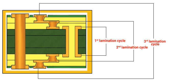 Real Quote Structure Breakdown (PCB Cost Breakdown)
To explain that the cost doubling isn't a "material issue" but a "process accumulation" issue, let's break down the underlying structure of a quote:
| Cost Item | 8-Layer Standard Board | 10-Layer HDI (1+N+1) | Reason for Cost Jump | | :--- | :--- | :--- | :--- | | Inner Layer Fabrication | 1x Baseline | 1.5x Baseline | Core layers and outer layers need separate fabrication and exposure | | Lamination Cycles | 1 time | 2 times (or more) | Initiates sequential lamination, machine time and labor double directly | | Drilling Technology | Mechanical Through-hole | Mechanical Buried Via + Laser Blind Via | High depreciation cost for laser machines; cost per hole multiplies | | Via Fill Process | None | Mandatory (Via Fill) | Blind vias need copper paste filling and planarization for SMT | | Back-drill | Depends on signal | Very High Probability Required | Removes stubs for high-speed signals, adds secondary machining |
The cost increase isn't because of two extra layers; it's because of "one extra lamination cycle."
Once you enter the realm of 10-layer boards, the system usually involves PCIe Gen4/Gen5 or serial data rates above 10Gbps. This triggers the third cost fault line: an insatiable demand for极致 physical tolerances and top-tier materials. Compounded by the continued tight supply of high-end materials in 2025, the pricing pressure on these types of boards intensifies further.
1. The Invisible Killer: Copper Roughness
When differential pairs operate in frequency bands above 10Gbps, high-frequency signals suffer significantly from the "Skin Effect," where current concentrates on the surface of the conductor. If the copper foil surface is too rough, the signal transmission path becomes like walking on a rugged mountain road, causing a sharp increase in resistance and Insertion Loss. High-speed signal studies indicate that above 1GHz, copper surface roughness can increase the effective resistance of a transmission line by up to 40%. To solve this, engineers must specify ultra-smooth copper foils (like HVLP), which significantly raises the baseline material cost.
 2. Dielectric Constant (Dk) Variation and PCB Impedance Control ±5%
High-speed signals are extremely sensitive to impedance matching. Tightening the allowable impedance tolerance from the standard ±10% to the stringent PCB Impedance Control ±5% demands not only perfect line width precision from the etching process but also不允许 any non-uniformity in the laminate's Dielectric Constant (Dk). In mass production, demanding such extreme ±5% tolerances leads to a cliff-like drop in yield. To compensate for scrap losses, manufacturers typically add a Scrap Compensation fee of $5 to $12 per board for small batch productions.
What truly sends the quote for a 10-layer board into the stratosphere is never the few millimeters of copper foil, but the "tolerances" that challenge the limits of physics.
Since HDI PCBs are so expensive, shouldn't we stubbornly stick to traditional multi-layer boards and absolutely avoid blind vias? This is the most common思维陷阱 hardware teams fall into. When faced with extremely congested routing scenarios (the Blind Via vs Through Hole dilemma), skillfully applying HDI technology can actually achieve the surprising strategic goal of "layer reduction."
Imagine a dense 0.4mm pitch BGA with hundreds of pins. If you insist on using traditional through-holes for fan-out, the sheer number of large vias acts like thick pillars piercing through the entire board, severely blocking all inner layer routing channels. To find paths for the remaining signals, engineers are forced to keep adding layers, ultimately pushing a design that could have been 6 layers into an 8-layer or even 10-layer structure.
The counter-intuitive breakthrough is this:
If, early in the design, you decisively add laser blind vias on the outer layers (a 1+N+1 HDI structure). These tiny blind vias only reside on the surface; they don't penetrate all the way through, instantly freeing up vast routing space on all the inner layers below. A design originally forced into 8 to 10 traditional layers due to blocked channels can be easily compressed back into a 6-layer or even 4-layer HDI structure.
Although introducing laser blind vias increases the process cost per layer, successfully eliminating several layers of expensive high-frequency material and reducing overall board thickness can actually lead to a significant decrease in the total mass production BOM cost.
HDI never exists purely for "increasing layers." Skilled engineers use HDI to "control the layer count."
Faced with rapidly evolving technical specifications, under what specific hardware conditions should a project team decisively choose to jump to a higher layer count stackup? Below is a "Layer Escalation Decision Model" crafted specifically for PMs and R&D managers, transforming the article's knowledge into a practical decision-making tool.
| Core Hardware Trigger Condition | Recommended Stackup Architecture | Expected Cost Magnitude | Key Decision Point | | :--- | :--- | :--- | :--- | | DDR4 / Signals < 5Gbps | 6-Layer Standard Board | Baseline Budget | Traditional single lamination, best cost-performance | | PCIe Gen4 / 10Gbps High-Speed Serial | 8-Layer Standard Board | 1.3 ~ 1.5x Baseline | Needs extra solid ground planes for signal shielding | | BGA Ball Pitch ≤ 0.4mm | 8-Layer HDI (1+N+1) | > 2.0x Baseline | Blind vias are mandatory; evaluate if this allows layer reduction | | Multiple Power Domains + < 1mm Thickness Limit | 10-Layer Advanced HDI | Deep Water Zone (Doubles) | Limits of sequential lamination;必须 meticulously calculate need for ±5% impedance |
If you are a PM or Procurement, upon receiving the initial architecture diagram from R&D, immediately perform the following checks. If your design hits any three of the following items, immediately request manufacturer involvement for a DFM (Design for Manufacturing) assessment; otherwise, mass production quotes will definitely spiral out of control:
In the race for advanced electronic hardware, cost control is never about meaningless price haggling with suppliers over a quote. It's about accurately avoiding the无效 deep waters that cause costs to explode during the "design phase" of the hardware architecture.
At eCloud, we don't just sell boards. We sell the architectural capability to "prevent layer count runaway." As an expert provider of local rapid prototyping and small-volume manufacturing services in Taiwan, eCloud PCB has built an efficient online platform specifically for R&D engineers, fully supporting advanced multi-layer and HDI processes. When evaluating designs above 8 layers, our engineering team proactively safeguards clients by:
If you are currently facing an R&D bottleneck, pressured by a quote explosion jumping from 8 to 10 layers, troubled by yield assessments for blind vias and sequential lamination, or watching high-frequency material costs spiral out of control, feel free to upload your design files to the eCloud PCB platform at any time. Let us, at the very front end of architecture definition, help you forge a successful product with顶尖 performance and absolute price competitiveness.
