March 5, 2026
When line width and spacing approach 30/30μm, the question is no longer “can it be done?” but rather— traditional HDI has reached its physical limits. As side etching begins to compromise impedance control, and as 5G and AI SoCs run out of escape routes for routing, Substrate-like PCB (SLP) is no longer an exclusive feature of flagship devices. It has become an inevitable choice for mid-to-high-end products. Recent hardware teardowns and supply chain dynamics reveal a major industry shift: high-end processes are rapidly trickling down. This paradigm shift, permeating from the pinnacle of the pyramid into the mainstream market, profoundly impacts the product layout decisions of every Project Manager (PM), procurement expert, and R&D Engineer (RD). We will uncover the underlying logic behind this technological shift through three manufacturing fault lines.
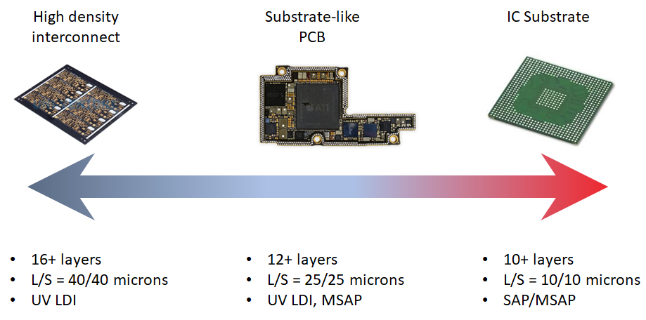
When discussing the challenges of miniaturization engineering, we must confront why traditional printed circuit board processes are encountering a physical fault line at this moment.
The traditional Subtractive Process relies heavily on chemical etching to remove unwanted copper layers. However, chemical etching possesses an unavoidable physical characteristic: Isotropy. When the target Line/Space (L/S) shrinks to 30/30μm or even lower, the etchant, while dissolving the copper vertically, inevitably also aggressively attacks the sides of the traces, causing Undercut.
This excessive undercut effect results in the residual copper traces having a trapezoidal cross-section instead of the ideal vertical rectangle. In high-speed signal transmission environments, a trapezoidal cross-section severely disrupts the Impedance Control of high-frequency signals and significantly increases the risk of micro-shorts or open circuits between adjacent微细 traces. Especially when dealing with new-generation AI SoCs (such as顶级 processors with package solder ball pitches shrinking to 0.8mm or even below 0.65mm), engineers must use traces below 30μm to achieve BGA Escape Routing within extremely confined spaces. At this point, the subtractive process not only suffers from poor yield but also becomes a primary cause of signal attenuation.
In a nutshell: When line widths go below 30μm, the subtractive process begins to lose control.
To address the need for micro-fine traces, the packaging substrate industry has long employed the Semi-Additive Process (SAP). SAP offers exceptional miniaturization capability, easily achieving 10/10μm line/space or even lower. However, the SAP process requires building upon a纯粹的 dielectric layer, demands extremely high cleanroom cleanliness, and necessitates massive capital investment in专用 equipment. Its high cost makes it difficult to大规模普及 on mass-market consumer electronic motherboards like smartphones.
Caught between the physical limits of HDI and the cost ceiling of SAP, the modified Semi-Additive Process (mSAP) emerged as a compromise yet efficient solution. mSAP starts with a copper-clad laminate featuring an ultra-thin copper foil. The subsequent process logic combines characteristics of both additive and subtractive methods: after defining patterns using photolithography, selective plating increases copper thickness, and finally, the ultra-thin base copper seed layer is removed by Flash Etching.
mSAP preserves a nearly vertical trace sidewall profile, which is crucial for complex SoC package escape routing and impedance matching. But we must clarify a core concept:
mSAP is not about chasing 10μm; it's about stabilizing 20μm.
It allows manufacturers to leverage existing high-volume equipment and cross the 30μm physical chasm in the most commercially beneficial way.
Implementing SLP is not merely about filling a specification sheet with smaller line width numbers; it's about system-level three-dimensional space restructuring.
The ultra-high routing density achieved through the mSAP process (e.g., 20/20μm L/S) grants hardware designers immense flexibility. This means that under the same architecture, the total layer count of the PCB and the motherboard area can be significantly reduced. A smaller motherboard not only lowers the overall device weight but also frees up valuable vertical space for the massive camera modules (DECO) in modern smartphones, or争取 to更大 battery capacity for power-hungry AI computing platforms.
This system-level dividend has already been proven in the终端 market. Within the Android camp, Xiaomi's 14 series and 15 series (such as the 15S Pro equipped with the latest 3nm chip Xring O1) extensively use substrate-like PCB (SLP) designs for their main boards, greatly simplifying internal structure and freeing up space, allowing camera modules and超大 capacity batteries to coexist perfectly. Similarly, Samsung has begun introducing advanced interconnect technology in its mid-range models like the Galaxy A55 5G, granting mid-to-high-end products the same flagship-level system space dividends.
In the microscopic battlefield below 30μm, the challenge for R&D teams lies in maintaining极致 physical stability, rather than endlessly stacking experimental data.
Regarding dielectric layer selection, low CTE (Coefficient of Thermal Expansion) and Low Dielectric Loss resins become critical. To meet the high-frequency transmission demands of 5G mmWave and AI edge computing, materials must possess excellent electrical properties to minimize signal transmission loss. Simultaneously, to withstand multiple Sequential Lamination cycles and the high temperatures of lead-free processes, high Tg (above 180°C) materials have become standard.
Preserving essential physical characteristics and eliminating redundant chemical experiments is the core principle for rapidly advancing project implementation.
For procurement experts responsible for supply chain布局 and capital expenditure, upgrading an mSAP production line is not a typical equipment purchase; it's a brutal淘汰赛. Expanding traditional HDI capacity might only require adding a few drilling machines. However, to stably mass-produce substrate-like boards with L/S below 30/30μm, one must cross extremely high capital barriers:
This is why 30/30μm is not a "design problem," but a "capital problem."
From a Project Manager's perspective, implementing SLP is undoubtedly a double-edged sword. Its high initial R&D and manufacturing costs must be justified through a system-level accounting logic to maximize commercial benefits.
The core logic of the accounting is: SLP costs more per layer, but requires fewer total layers.
We must understand that one of the biggest cost drivers in multi-layer board manufacturing is "Sequential Lamination." Each additional lamination cycle requires placing the panel back into an expensive press, undergoing lengthy heating and cooling processes. This is not only a capacity bottleneck but also accompanied by progressively decreasing yield rates.
For example, a complex motherboard originally requiring 14-layer Any-layer HDI, if重新 routed using SLP technology, could potentially be completed in only 10 layers thanks to the 20/20μm ultra-high routing density. These 4 fewer layers mean saving significant sequential lamination time and scrap risk. Through a "quality over quantity" design strategy, PMs can deliver clear system dividends for the product:
让老板与决策层看到这份宏观的“系统红利”,才是推动高阶制程导入的最强说服力。 (Making senior management and decision-makers see this macroscopic "system dividend" is the most powerful persuasion for driving the adoption of advanced processes.)
With the普及 of AI terminal hardware and the rise of next-generation devices, the maturation of technology and the downward渗透 of advanced processes are irreversible industry trends. However, amidst this wave, blindly chasing miniaturization numbers is not the optimal solution.
In eCloud's high-end motherboard projects, when evaluating whether to implement SLP, we don't just look at the line width numbers; we assess:
✔ Whether the limits of the subtractive process are being approached
✔ Whether layer count stacking is leading to lamination risks
✔ Whether mSAP can be used to achieve layer count reduction
Because true competitiveness, lies not in who can achieve 20μm, but in who knows— when 20μm is truly necessary.
