I. What are PCB Stamp Holes?
Stamp holes refer to holes designed on a circuit board panel that connect the small PCBs forming the array, allowing you to easily separate the individual boards from the panel.
Stamp holes are a perforated design; when you press down, they break, enabling you to remove or separate the circuit boards without damaging the PCB itself.
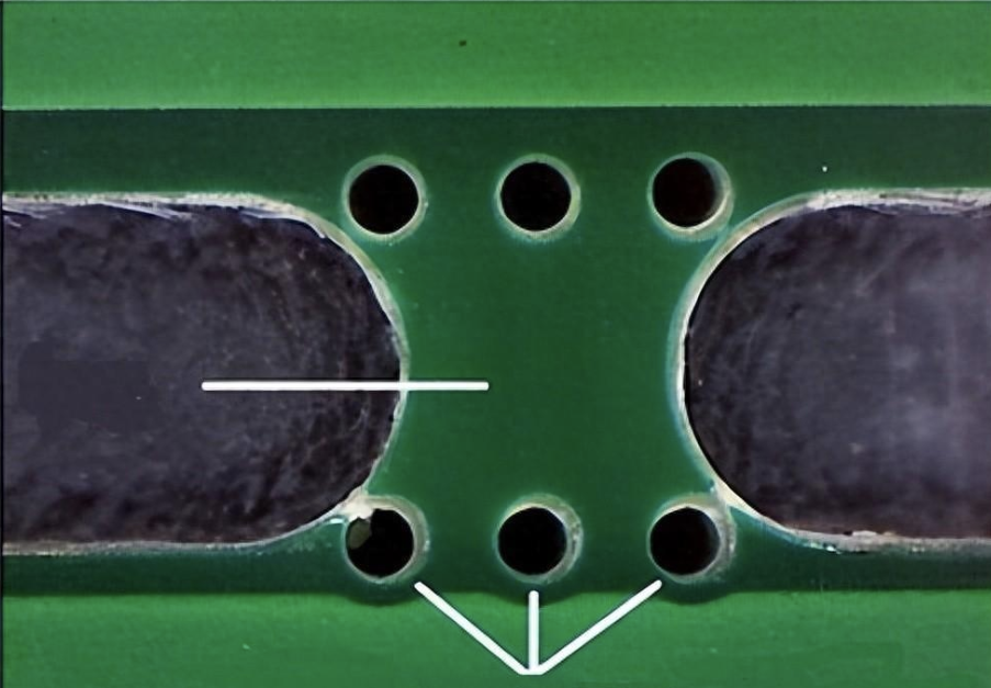 [Image: Schematic diagram of PCB stamp holes]
II. The Purpose of PCB Stamp Holes
There are several reasons for designing stamp holes on a PCB, mainly including the following two:
- Connecting small PCBs into a group: When you have a number of PCBs that need to be connected but are too small to use connectors, stamp holes can be used to link them together. The perforations allow current to flow through the PCB and connect to other nearby PCBs.
- Transmitting power and data between two different PCBs or devices: If you need one device to communicate with another, stamp holes serve as an excellent bridge.
III. PCB Stamp Hole Design Requirements
When designing stamp holes, several physical dimension standards require special attention:
1. Number of Stamp Holes
Stamp holes are typically grouped in sets of five to connect boards together, though the exact number may vary depending on your PCB design requirements.
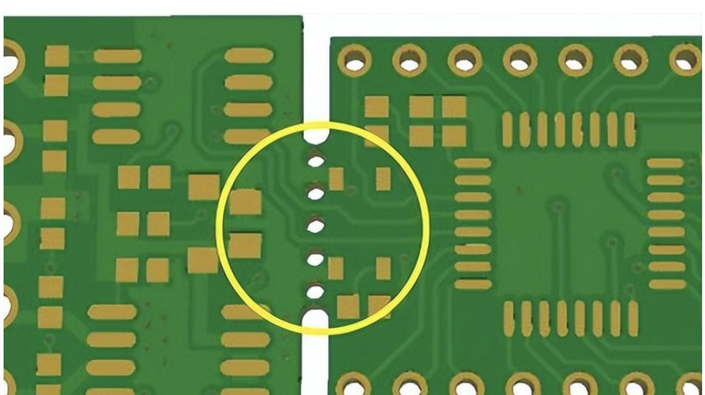 [Image: PCB stamp hole count]
2. Stamp Hole Size
The size of stamp holes is typically 0.020 inches or 0.5 mm in diameter. This dimension is not absolute; the most suitable size is determined by the thickness of the laminate used to manufacture the PCB.
 [Image: PCB stamp hole size]
3. Stamp Hole Pitch
Typically, the pitch for PCB stamp holes is 0.030 inches or 0.76 mm. Maintaining an appropriate pitch prevents components from being placed too close together, which could lead to short circuits.
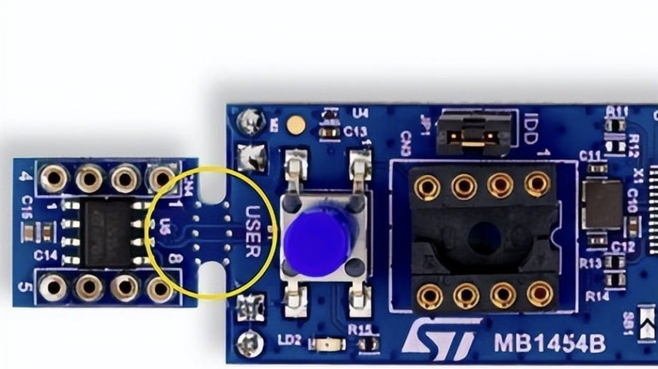 [Image: PCB stamp hole pitch]
IV. 4 Tips for Designing PCB Stamp Holes
To ensure smooth production and avoid damaging the board, be sure to master the following 4 design tips:
- Reserve sufficient connecting tabs to support the PCB: Because stamp holes are open-hole designs, insufficient connection between boards can lead to structural issues. Ensure the connecting tabs are strong enough to support the weight of components on the board.
- Keep away from sensitive components: They must be kept away from sensitive components! Breaking the connecting tabs can generate mechanical stress that may cause damage, potentially leading to electrical shorts.
- Spacing between two sets of stamp holes should be between 60mm and 90mm: Too much space weakens the board structure, making SMT placement difficult; too little spacing allows solder to flow to other areas, causing shorts.
- Maintain a safety distance of at least 0.125 inches from the nearest component: The closer to a component, the harder it is to solder and secure. Insufficient distance also increases the risk of solder bridges forming between pads or traces, which is especially important for high-density PCBs.
V. Differences Between PCB Stamp Holes and V-Cut
In panel design, V-Cut and stamp holes are the two most commonly compared methods:
1. V-Cut
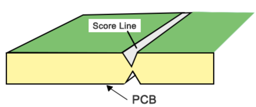
V-Cut is the most common panelization method for PCB assembly. After combining multiple boards, a V-Cut machine cuts V-shaped grooves between the boards, allowing them to be broken apart during use or before packaging. For double-sided V-Cut, the depth should be controlled to approximately 1/3 of the board thickness (sum of groove depths on both sides).
- Advantages: Lower cost, easier to manufacture, better quality, and less prone to deformation.
2. PCB Stamp Holes
In many irregular-shaped designs, PCB stamp holes are used instead of V-Cut.
- Advantage 1 (Direct breakability): They offer better strength and can be broken directly, unlike some connecting tabs that require router equipment for cutting.
- Advantage 2 (Better structural adhesion): The larger the opening, the greater the surface area for adhesive to grab, making mounting and fixing easier and preventing the PCB from moving during processing.
VI. IPC-7351 Standard Reference for Stamp Holes
The industry typically refers to the IPC-7351 standard to evaluate whether stamp hole designs are acceptable:
- Preferred Design: Traces must be at least 1 mm away from the PCB edge and the stamp holes.
- Acceptable Design: Traces placed near the top of the PCB edge and stamp holes are acceptable, provided the trace routing direction is correct and there is no insufficient routing space.
- Not Recommended Design: Routing traces flush with the finished board edge and the mouse bites (the fractured area of the stamp holes) is strongly discouraged, as it is highly likely to lead to subsequent soldering and reliability issues.
