March 26, 2026
As BGA and SMD chip packages continue to shrink in size, traditional wiring methods have reached their limits. This has led to the widespread adoption of **Via-in-Pad (often referred to in the industry as “in-pad vias”)** technology. Today, we will take an in-depth look at the principles, appropriate applications, and manufacturing processes of Via-in-Pad.
Via-in-Pad, as the name suggests, is a design where a via is placed directly on the pad of a surface mount device (SMD). This approach allows interlayer connection directly within the pad, significantly saving board space.
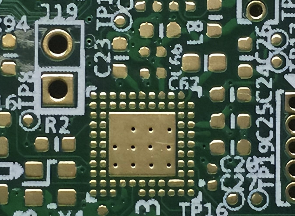
In a standard via design, the signal is routed from the pad with a short trace before connecting to the via. This allows a solder mask to be applied between the pad and the via, preventing solder paste from wicking into the via during reflow, which could lead to insufficient solder and poor joints.
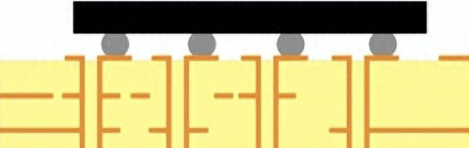
In a Via-in-Pad design, the drilled hole is located directly inside the pad, making it impossible to use a solder mask to block solder loss. The industry standard solution is to use the POFV (Plated Over Filled Via) process, where the hole is filled with resin, plated over, and planarized, leaving a flat, conductive pad surface.

When evaluating whether to use Via-in-Pad, consider whether your design meets the following requirements:


Attempting to route a 0.5mm pitch BGA package using traditional methods often results in DRC (Design Rule Check) errors due to constraints on trace width, annular ring, and drill size. For these fine-pitch components, using plated and planarized Via-in-Pad is the most efficient approach.
Signals can directly enter the inner layers vertically, minimizing the need for surface layer routing. This allows bypass capacitors to be placed as close as possible to the IC, minimizing parasitic inductance, shortening power and ground return paths, and effectively reducing EMI radiation in high-frequency designs.
It is essential to ensure that the via within the pad meets the manufacturer's minimum annular ring requirements. If the BGA pad diameter is smaller than the combination of the via diameter plus annular ring, it is recommended to use a Solder Mask Defined Pad (SMD) design.
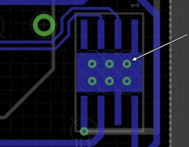
For the bottom ground pad of QFN packages or the thermal pads of high-power components, multiple thermal vias are often used. In these cases, the vias do not always need to be fully filled and plated over, but care must be taken as outgassing and voiding during reflow can cause component tilting. If the budget allows, filling these thermal vias provides better thermal conductivity and coplanarity.
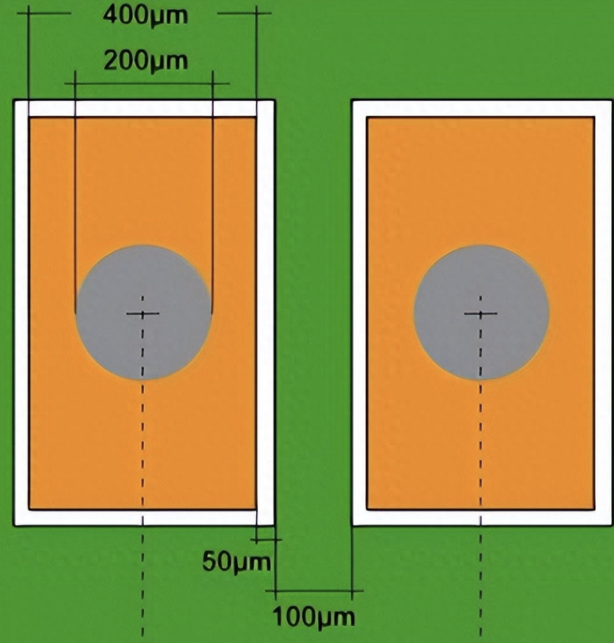
Generally, the typical minimum pitch for a Via-in-Pad solution is approximately 600μm (including: minimum 200μm drill diameter, minimum 400μm pad size, 50μm solder mask clearance, 100μm solder mask web). If laser-drilled microvias are used, the drill diameter can be reduced to 100μm, allowing a pitch of 500μm or even smaller.
To achieve a perfect Via-in-Pad, the PCB manufacturer must go through a more complex sequence than standard boards:
Drilling ➔ Plating ➔ Selective Plugging ➔ Curing ➔ Planarization/Polishing ➔ Plating over via ➔ Etching ➔ Solder Mask Application.
By hiding the via directly under the contact pad, Via-in-Pad offers hardware engineers and layout designers unparalleled spatial flexibility. Compared to traditional vias, it provides the following absolute advantages:
