January 8, 2026
Driven by AI servers and automotive electronics, PCB design has transformed from simple "connect-the-dots" to a precise physical game. For Layout Engineers, the challenge in 2025 is: how to hold the "red line" of yield while keeping costs under control. This report focuses on three key areas: 3mil trace width, annular ring calculation, and teardrop design, analyzing why these parameters determine the life or death of a product.
Why do factory sales reps often say, "4mil/4mil is standard, 3mil/3mil costs extra and has low yield"? This isn't just an equipment issue; it's a physical limitation of fluid dynamics.
In CAD software, lines are perfect rectangles; but in the factory's etching tank, the chemical solution attacks "omnidirectionally." As the solution corrodes the copper foil downwards, it also attacks sideways, forming a trapezoidal cross-section.
F = T / X (T = Copper Thickness, X = Undercut amount).DfM Recommendation: Unless it is a BGA Fan-out area, try to maintain 4mil/4mil or above for the entire board. If 3mil trace width is mandatory, be sure to reduce copper thickness to 0.5 oz or 1/3 oz.

The annular ring is the ultimate victim of accumulated errors in PCB manufacturing. Many RDs only look at the finished hole size but ignore the cumulative effects of "Drilling Tolerance" and "Layer-to-Layer Registration."
Don't set Pad Size by feel; apply the formula:
L = a + 2b + c
In Taiwan's mass production factories (e.g., Unimicron, Tripod), the tolerance c for multilayer boards is at least 8~10 mil. This includes:
Practical Case: If you want an 8mil finished hole (Via):

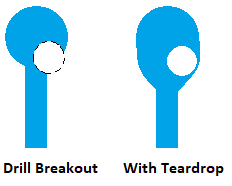
In high-density designs of 2025, teardrops are no longer "optional" but "standard."
Teardrops increase the copper area at the junction of the trace and the pad.
Many RDs worry that teardrops affect Signal Integrity (SI). In fact, modern EDA tools support "Snowman" or smooth curve teardrops, and their impedance discontinuity is far less than the risk brought by "via cracking."
Conclusion: For IPC Class 3 products or multilayer boards above 10 layers, be sure to enable the teardrop function.
Taiwan's PCB industry leads the world technologically, but different manufacturers have different "Capabilities" and "Optimal Cost Points."
| Manufacturer Type | Representative Manufacturers | Technical Red Line (Mass Production Level) | DfM Strategy | | :--- | :--- | :--- | :--- | | High-End HDI / Substrate | Unimicron, Compeq | Trace Width < 2mil<br>Microvia 3mil | Suitable for AI servers, Apple-grade products. Requires mSAP process, high cost. | | Multilayer / Automotive | Tripod | Trace Width 3~4mil<br>Annular Ring Class 3 | Suitable for server motherboards, automotive radar. Focus on CAF protection and heavy copper control. | | General / Quick Turn | (Various SMEs) | Trace Width > 5mil<br>Pad > 20mil | Suitable for consumer electronics. Do not challenge limit parameters, or yield will drop below 80%. |
Mastering these red lines means you are designing not just a circuit diagram, but a product that can be manufactured with high quality.
