In the highly mature Electronics Manufacturing Services (EMS) and Printed Circuit Board (PCB) supply chain—ranging from IC design in Hsinchu Science Park to the PCB manufacturing clusters in Taoyuan and New Taipei City—Design for Manufacturing (DFM) is no longer just an engineering specification. It is a core strategy determining profit structures and market competitiveness.
For R&D engineers, Layout engineers, and future electromechanical professionals, understanding the physics and economic logic of Panelization is a mandatory prerequisite for bridging the gap from "lab prototype" to "million-unit mass production."
Panelization is not merely a geometric game of arranging a single Unit repeatedly; it is a multidimensional tradeoff involving material mechanics, thermodynamics, fluid dynamics (solder paste printing), and automation control. An optimized panel design can boost Surface Mount Technology (SMT) production efficiency by over 30% and keep material waste below 15%. Conversely, poor design results in low material utilization and can introduce mechanical stress during Depaneling, causing Micro-cracks in Multi-Layer Ceramic Capacitors (MLCCs), leading to catastrophic failures in the end market.
This report provides a comprehensive technical guide analyzing the two mainstream PCB panelization technologies—V-Cut and Mouse Bites (Stamp Holes)—across four dimensions: mechanical processing principles, cost structure analysis, SMT line dynamics, and reliability engineering. We will explore when to choose V-Cut for ultimate cost efficiency, when to compromise with Mouse Bites for design freedom, and how to maximize material utilization through precise mathematical calculations.
2. Mechanical Principles and Design Specs: V-Cut Technology
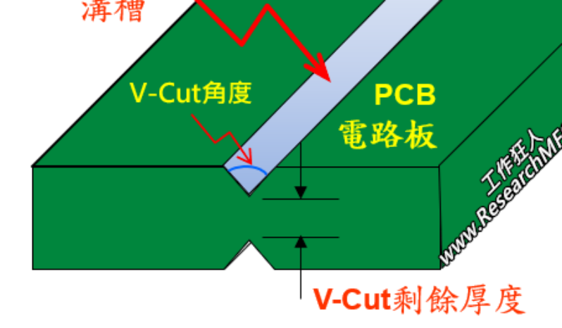
V-Cut, also known as V-Scoring or V-Groove, is the most mature and widely used separation technology in the PCB industry. Essentially, it is a subtractive process of "pre-stress concentration," creating structural weaknesses via mechanical cutting to facilitate controlled separation by external force.
2.1 Machining Mechanism and Web Thickness Control
2.1.1 Cutting Dynamics and Geometry
V-Cut is typically performed in the latter stages of PCB fabrication (after surface finish, before routing). It uses two opposing rotating Tungsten Carbide circular blades cutting simultaneously from the Top and Bottom along a linear path.
- Cutter Angle: Industry standards include 30°, 45°, and 60°.
- 30° Cutter: Creates the narrowest kerf, occupying minimal surface copper clearance. It is the preferred choice for HDI (High Density Interconnect) boards but has a fragile tip, faster wear, and demands high precision in depth control.
- 45°/60° Cutters: Wider kerf, longer tool life, and leaves a larger chamfer after separation (better tactile feel). Common in consumer electronics.
- Web Thickness: V-Cut does not sever the board; it retains a core layer called the "Web." For a standard 1.6mm FR-4 board, the residual thickness is usually controlled at 0.4mm ± 0.1mm.
- Mechanical Balance: If the web is too thin (<0.25mm), the panel may suffer from Sagging due to material softening above the glass transition temperature (Tg) during SMT reflow (>240°C), or break during transport. If too thick (>0.6mm), the mechanical stress required for separation rises exponentially, causing delamination or solder joint cracking.
2.1.2 Jump Scoring: Breakthroughs and Limitations
Traditional V-Cut requires a "cut through from start to finish" due to the blade's rotation radius. However, modern CNC V-Cut machines introduce Jump Scoring.
- Principle: The cutter head features Z-axis servo control, allowing the blade to lift over specific areas and drop back down to continue cutting.
- Application: Useful for designs with external interfaces (e.g., HDMI, RJ45) protruding beyond the board edge, or when retaining stiffeners is necessary for panel rigidity.
- Cost: Jump Scoring significantly reduces the Feed Rate and increases programming complexity. PCB fabs typically charge an NRE (Non-Recurring Engineering) fee or increase the unit price for this process.
2.2 V-Cut Design Constraints and DFM Specs
Despite its cost advantages, V-Cut imposes strict geometric limitations:
- Linear Constraint: V-Cut can only travel in straight lines. For circular, L-shaped, or T-shaped outlines, it cannot define the shape alone and must be combined with Routing.
- Keep-out Zone & Stress: The area near the V-Cut line is the "epicenter" of depaneling stress.
- Copper Clearance: Inner/Outer copper must be at least 0.5mm (rec. 1.0mm) from the V-Cut center. Proximity risks tearing copper or altering impedance.
- Component Clearance: SMD components should be >1.0mm from the line. Tall components (electrolytic caps, transformers) need 3.0mm - 5.0mm clearance to prevent collisions with the depaneling machine's Blade Guard.
- Asymmetric Cutting Risk: If the top and bottom cut depths are unequal (e.g., Top 0.8mm, Bottom 0.4mm), cracks will not propagate vertically but deflect toward the shallower cut, causing severe burrs or structural damage. Alignment Tolerance within ±0.05mm is a key capability indicator for PCB fabs.
3. Mechanical Principles and Design Specs: Mouse Bites (Stamp Holes)
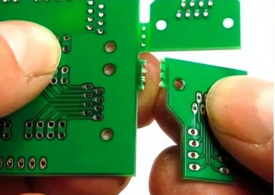
When V-Cut's linear restrictions fail to meet complex shaping needs, Mouse Bites (formally Tab Routing) become the essential solution. This involves using a CNC Router to mill away most of the outline, leaving small connection bridges (Tabs) drilled with a series of holes to simulate a stamp's perforation line.
3.1 Geometric Mechanics
Designing Mouse Bites is an art of balancing "Connection Strength" vs. "Depaneling Difficulty."
3.1.1 Golden Rules for Drilling
- Hole Diameter: Recommended standard is 0.5mm (20mil) to 0.8mm (32mil).
- Analysis: Too large (>1.0mm) weakens the tab, risking detachment during Wave Soldering. Too small (<0.4mm) fails to guide crack propagation, leaving large protrusions, and increases cost due to drill bit breakage.
- Pitch: Center-to-center distance is usually Diameter + 0.3mm to 0.4mm. (e.g., 0.5mm holes with 0.8mm pitch leave a 0.3mm solid web). This tiny web is the key stress release point.
- Arrangement: Typically 3 to 5 holes per Tab.
3.1.2 Recessed Design and Burr Control
Mouse Bites inevitably leave jagged edges (Burrs) after separation. To prevent these from interfering with mechanical housing assembly:
- Design Rule: The center of the Mouse Bite holes should be recessed 0.2mm - 0.5mm inside the board outline.
- Advantage: Burrs remain within the standard dimensions, eliminating the need for manual Sanding—a crucial factor in reducing labor costs at assembly plants.
3.2 Routing Paths and Material Removal
- Router Bit: Standard diameters are 1.6mm, 2.0mm, or 2.4mm.
- Gap Requirement: A gap of at least 2.0mm must be left between boards for the cutter path. Compared to V-Cut's "zero gap," this is an inherent material utilization disadvantage.
- Processing Time: Routing is much slower than V-Scoring and requires tracing the full perimeter. This translates to higher Machine Hour Rates.
4. V-Cut vs. Mouse Bites: Comprehensive Decision Matrix
To assist R&D in DFM decision-making, we compare the two based on cost, mechanics, and application.
4.1 Comparison Table
| Dimension | V-Cut (V-Scoring) | Mouse Bites (Tab Route) | Engineering Insight |
| :--- | :--- | :--- | :--- |
| Machining Cost | Low | Medium/High | V-Cut is a fast linear pass; Routing requires slow CNC milling/drilling. Router bits cost more than V-cut blades. |
| Material Utilization | Very High (~100%) | Medium (85-90%) | V-Cut allows 0mm spacing; Mouse Bites need >2mm gaps. Significant waste on small boards. |
| Edge Quality | Smooth | Rough (Jagged) | V-Cut edges are smooth but have glass fiber strands; Mouse Bites leave burrs (requires recessed design). |
| Shape Limit | Linear Only | Any Shape | V-Cut cannot handle arcs/notches; Mouse Bites are the only solution for irregular shapes. |
| Structural Rigidity | High | Low | V-Cut retains a continuous spine; Mouse Bites rely on point connections (large panels may sag). |
| Depaneling Stress | High (if manual) | Low (if routed) | Manual snapping of V-Cut creates massive stress; Mouse Bites can be nipped or routed with controlled stress. |
4.2 Case Studies
-
Scenario A: Mass Production Rectangular IoT Module
- Choice: V-Cut.
- Reason: Perfect for rectangular shapes. 0mm spacing increases yield per 18"x24" panel by 10-15%. Lowest cost.
-
Scenario B: Circular Smartwatch PCB
- Choice: Mouse Bites (Tab Route).
- Reason: V-Cut cannot cut circles. Must use CNC routing with 3-4 tabs connecting to the process rail. Tabs must avoid connector areas.
-
Scenario C: Control Board with Overhanging USB & Side Buttons
- Choice: Hybrid.
- Reason: Use V-Cut on short edges (no overhangs) for rigidity; use Routing (Mouse Bites) on long edges to mill out space for the USB.
5. Material Utilization: Avoiding the "More Waste than Board" Trap
Material Utilization is a hidden leverage point in PCB procurement. Since Copper Clad Laminates (CCL) come in standard sizes, poor dimensioning leads to massive waste.

5.1 Standard Working Panels
In the Taiwan/Asia supply chain, mainstream CCL sizes include:
- 18" x 24" (457mm x 610mm): Most universal.
- 21" x 24" (533mm x 610mm): Common for multilayers/high volume.
- Usable Area: After deducting Panel Margins (10-15mm per side for handling/tooling), an 18x24 panel effectively offers a 16" x 22" (406mm x 558mm) working area.
5.2 Calculation Logic
- Multiplier Effect:
- Design A: Width 50mm -> Fits 8 cols -> 0mm waste.
- Design B: Width 51mm -> Fits 7 cols -> 43mm waste.
- Conclusion: A 1mm increase can drop output by 12.5%. Always consult the fab's matrix before finalizing dimensions.
- Nesting & Interlocking:
- For L-shaped or T-shaped boards, standard arrays create huge internal waste.
- Solution: 180° Interlocking. Nesting the protrusion of one board into the recess of another can boost utilization from 60% to over 80%.
6. Risk & Quality Control: MLCC Cracking & Stress Management
This is the "silent killer" in PCB panelization.
6.1 MLCC Flex Cracking Mechanism
MLCCs are brittle. When a PCB bends or twists during depaneling, stress transfers to the MLCC terminals. If tensile stress exceeds the ceramic's limit, a 45° latent crack forms.
- Danger: These cracks often pass ICT/FCT testing but fail in the field due to moisture ingress or thermal cycling, causing short circuits.
6.2 Orientation Strategy
- Rule: Align the long axis of the MLCC Parallel to the V-Cut/Break line.
- Why: When the board bends along the cut, the stress is perpendicular to the bend axis. Parallel alignment minimizes the tension pulling the capacitor ends apart.
- Bad Design: MLCC long axis Perpendicular to the V-Cut line. This maximizes risk.
6.3 Depaneling Process Selection
- Manual Break: Highest stress. Prohibited for automotive/high-reliability products.
- Pizza Cutter (Blade): Moderate stress. Good for V-Cut.
- Router Depaneling: Lowest stress (near zero). Best for Mouse Bites and sensitive components, though equipment is expensive.
7. Process Edge (Break-away Rail) Details
The rail is the PCB's "coordinate system."
- Width: Standard 5mm (up to 8-10mm if components are near the edge).
- Fiducial Marks: 1.0mm solid copper dot with 2.0mm solder mask opening. At least 3 points in an "L" configuration for machine vision/alignment.
- Tooling Holes: 2.0mm or 3.175mm Non-Plated Through Holes (NPTH) for test fixtures.
- ESG: V-Cut reduces rail width requirements, lowering waste (copper/resin/fiberglass), aligning with environmental goals.
9. Conclusion: The R&D Decision Checklist
Panelization is the starting point of DFM and the deciding factor in cost control.
Decision Matrix:
- Shape Check: Rectangular -> V-Cut. Irregular -> Mouse Bites.
- Cost Check: High volume, price-sensitive -> V-Cut (aim for 0mm spacing).
- Stress Check: MLCC/BGA near edge -> Mouse Bites + Router Depaneling OR V-Cut + Jump Scoring + Increased Keep-out.
- Interface Check: Overhanging components -> Mouse Bites + Milled slots.
Pro-Tips for Cost Saving:
- Calculate First: Ask the fab, "What dimensions fit best on an 18x24 panel?" before routing.
- X-Outs: Allow "X-out allowed" (shipping panels with bad units marked). Demanding "100% good panels" increases board cost by 10-20%.
- Standardize Rails: Use consistent rail designs across projects to reuse test fixtures and save NRE.
For engineers, mastering these details is not just about saving the company money—it's about designing products that are Manufacturable, High Quality, and Competitive. Panelization is the bridge between design ideals and mass production reality.
