May 29, 2026
Hardware R&D and PCB Layout engineers have likely fallen into this trap: the design looks flawless, simulations pass with flying colors, and you confidently send it out for manufacturing and assembly, only to face a disaster during mass production. Either the BOM components don't match the PCB pads, causing placement offsets that make soldering impossible; or the silkscreen covers the pads and Mark points are missing, leaving SMT machines unable to recognize the board. Sometimes, trace width/spacing or drill clearances violate manufacturing rules, resulting in the fab house rejecting the design and requiring a spin. Worse yet, hidden short or open circuits can cause the finished board to burn up upon power-on, doubling rework costs and severely delaying the project schedule. The truth is, the vast majority of PCB mass production failures aren't caused by faulty circuit logic, but by inadequate Design for Manufacturability (DFM) verification. Many engineers focus heavily on circuit logic while neglecting manufacturing process validation, assuming the fab house or assembly plant will figure it out and release the board. Little do they know, a minor oversight in the design phase turns into a fatal, irreversible flaw in production. Skipping a comprehensive DFM check early on means spending ten times the effort cleaning up the mess later. Today, we've compiled a 16-point comprehensive DFM checklist that must be completed before sending your design to the factory. This covers eight core areas: design verification, manufacturing specifications, silkscreen labeling, SMT placement points, routing, drilling, solder mask dimensions, and electrical safety. We recommend hardware and layout engineers check these items one by one to avoid all mass production risks!
The foundation of PCB design isn't about how aesthetically pleasing the routing looks, but ensuring the design files, BOM, schematics, and netlist form a completely closed loop. If source parameters are misaligned, flawless downstream manufacturing processes won't save the board.
① Footprint Matching Check
All component models and footprint specifications in the BOM must perfectly match the pad dimensions on the PCB. It is strictly forbidden to have a situation where “component selection is updated, but the PCB pads are not synchronized.” We recommend two‑way confirmation between hardware and layout engineers to rectify any dimension or footprint mismatches immediately, preventing assembly failures at the source.
② Netlist Consistency and Document Layer Check
The schematic is the logic core, and the PCB is the physical carrier; the two must be fully synchronized. Import the latest netlist to compare routing and network relationships, preventing discrepancies like “schematic updated but PCB not” or vice versa. Simultaneously, ensure the document layer settings output in the Gerber files are entirely correct to avoid read errors at the fab house.
Any design that ignores the physical limits of the fab house’s capabilities is purely theoretical. Copper thickness and surface finish directly determine the durability and conductivity of the circuit board.
① Copper Thickness Verification
Strictly compare with the project’s initial requirements to ensure the copper thickness on each layer meets the standard. Insufficient copper leads to inadequate current‑carrying capacity and high‑temperature burnout; excessive copper increases etching difficulty and costs. Ensure the parameters fit the product’s power ratings and application scenarios.
② Surface Finish Check
Based on the actual application environment and assembly requirements, verify if the chosen surface finish is appropriate. Whether it’s HASL, ENIG, or Immersion Silver, it must match the requirements for moisture resistance, corrosion resistance, and solder joint strength, avoiding poor wetting or oxidation caused by improper selection.
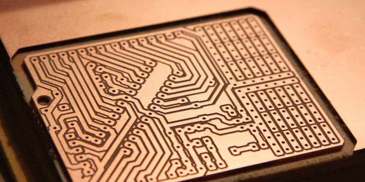
Silkscreen is not simply decoration; it is a critical indicator for SMT production, after‑sales maintenance, and product traceability.
① Silkscreen Manufacturability Check
All component designators must be legible. It is strictly prohibited for silkscreen to cover pads or solder mask openings, as this will impact soldering. The mandatory standard requires a silkscreen line width of ≥ 0.12 mm to prevent blurry or peeling text caused by overly thin fonts.
② LOGO and Functional Labeling Check
Necessary information such as version numbers, polarity indicators, and Pin 1 indicators must be prominent and standardized. This serves not only as brand identification but also as a clear guide for later assembly and debugging.
Modern PCBs rely entirely on automated assembly. Mark points and Pin 1 indicators are the baseline for precise machine recognition.
① Compliant Fiducial Mark Addition
Any surface containing SMD components must include standard optical Fiducial Marks. If Mark points are missing or under‑sized, the SMT machine cannot position the board, directly resulting in placement offsets or missing components.
② Pin 1 Indicator and Designator Check
Pin 1 for critical components like ICs, polarized capacitors, and diodes must be labeled accurately and visibly. Designators must be neatly arranged without overlapping to avoid reverse component placement and power‑on burnouts caused by unclear labeling.
① Trace Width and Spacing Check
The hard line: trace width and clearance must exceed the fab house’s minimum process capabilities (standard mass production recommends ≥ 4 mil). Never blindly compress these limits just to save space; doing so leads to broken traces during etching or shorts between adjacent lines, causing your yield rate to plummet.
② Critical Network Test Point Placement
Power, GND, and core signals must have standard test points strategically placed so that probes can make direct contact without blind spots or physical obstruction. This drastically improves the efficiency of post‑production power‑on testing and troubleshooting, eliminating the need for destructive board modifications.
Drilling is a high‑risk zone in manufacturing. Minor configuration errors can easily trigger board delamination or complete scrap.
① Drill Clearance and Via‑in‑Pad Check
Through‑hole spacing should strictly be maintained at ≥ 0.3 mm to prevent drill breakout or CAF (Conductive Anodic Filament) issues. Additionally, unless the manufacturing process allows for and includes resin plugging and over‑plating, strictly avoid Via‑in‑Pad designs to prevent solder wicking, which causes empty joints or hidden shorts.
② NC Drill and Route Layer Alignment
Ensure the parameters and coordinates of the NC Drill layer and the outline Route layer match perfectly to eliminate off‑center, incorrect, or missing holes.
③ Stub and Dangling Routing/Via Check
The board must be free of invalid, suspended routing or isolated vias. These redundant stubs act as antennas and can create acid traps that lead to micro‑shorts over time.
① Solder Mask Opening and Copper Exposure Check
Areas requiring exposed copper for heat dissipation or testing must be accurate and compliant. There must be no excessive solder mask openings that introduce short‑circuit risks, nor missing openings that prevent necessary soldering.
② Key Mechanical Dimension Tolerance Verification
The PCB outline, mounting holes, and mating slots must be strictly verified against the mechanical drawings for proper tolerances. This ensures seamless integration with the final enclosure – no jamming, no offsets.
After completing all visual and structural checks, this is the final line of defense before mass production.
PCB R&D is 70% circuit design and 30% DFM verification.
Don’t wait until you have to scrap boards and halt mass production to regret ignoring the details, and don’t assume DFM checks are a waste of time. Using this 16‑point comprehensive checklist, hardware and layout engineers should collaborate to pass/fail each item. Spending an extra half‑hour before releasing the design can save countless revision fees and crippling project delays later.
We highly recommend teams integrate this checklist into their standard SOP to eliminate all mass production risks right at the source!
