May 28, 2026
High-Definition Multimedia Interface (HDMI) is currently the most ubiquitous fully digital audio and video transmission interface in electronic products. Its core advantage lies in the ability to simultaneously transmit uncompressed high-definition video and multi-channel audio signals using a single cable, greatly simplifying system connectivity. From everyday TVs, set-top boxes, gaming consoles, and PCs to professional digital audio and automotive displays, HDMI is everywhere. However, under high-frequency transmission (up to 42.6 Gbps for HDMI 2.1), the quality of the Printed Circuit Board (PCB) design directly dictates Signal Integrity (SI) and Electromagnetic Interference (EMI) performance. This special topic will provide a comprehensive guide for hardware engineers, covering HDMI connector types, pin definitions, core Layout guidelines, and, most importantly, Design for Manufacturability (DFM) checkpoints.
HDMI signals do not require any D/A or A/D conversion before transmission, maintaining exceptional signal purity. When selecting components and routing your layout, it is essential to understand the five common connector types:


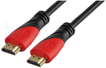
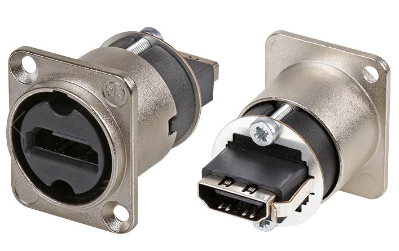
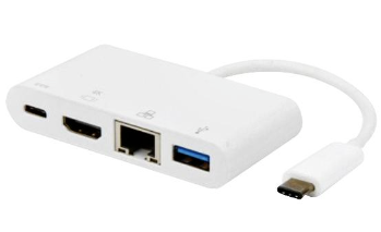
💡 Engineer's Tip: These HDMI interfaces are “not fully physically compatible” (e.g., Type A cannot plug into Type B). However, because Type A and Type C (Mini) differ only in physical dimensions while sharing identical pin definitions, they are perfectly compatible via passive adapter cables.
Taking the most common HDMI Type A as an example:
When a Source (e.g., a PC) and a Sink (e.g., a monitor) are connected via an HDMI cable, the hardware follows a clear handshake protocol:
To ensure the flawless transmission of high‑speed TMDS differential signals and prevent severe EMI issues, layout engineers must strictly adhere to the following guidelines:
Impedance and Skew Control
The PCB characteristic impedance standard for differential pairs is 100 Ω (±10%). To prevent phase shift, the length mismatch among the four differential pairs (Inter‑pair skew for Data x3, Clock) must be controlled within 10 mil. The length mismatch between the two traces of a single differential pair (Intra‑pair skew) must be less than 5 mil. The spacing (Air gap) between the four differential pairs should be kept at 15 mil or more to minimise crosstalk.
Reference Ground and Vias
High‑speed signals must be routed adjacent to a solid main GND plane, and crossing split planes is strictly prohibited. If layer transitions (vias) are necessary, Stitching Vias must be placed as close to the signal vias as possible to ensure an uninterrupted return path.
ESD Protection Component Placement
ESD protection devices must be placed as physically close to the HDMI connector as possible. It is imperative to use small‑package pull‑up resistors and ESD components, because smaller pads introduce less parasitic capacitance and lower impedance degradation.
Eliminate Stubs
Fine‑tuning matching resistors for signal lines should be placed near the receptacle. The traces should route directly through the pads of the ESD components and resistors to keep any resulting branch “Stubs” as short as possible.
A perfect layout is useless if the PCB fabrication house cannot manufacture it, or if the yield is unacceptably low. Before releasing your board for manufacturing, you must verify the following DFM items for HDMI interfaces:
Impedance Trace Process Margin
During fabrication, the manufacturing tolerance for impedance traces is tightly controlled at ±10% (standard traces are usually ±20%). Therefore, your designed width for impedance traces should ideally be larger than the manufacturer’s “minimum process limit” to leave an adequate safety margin, preventing impedance failures due to over‑etching.
Solder Mask Openings and Solder Mask Dams
The pin pitch of HDMI connectors is very dense. Whether using SMD or Through‑Hole (DIP) pins, absolutely no solder mask openings should be missed. More importantly, the “Solder Mask Dam” between adjacent pads must be greater than 4 mil. If the dam is too narrow, the manufacturer cannot print the green solder mask web between the pads, which highly increases the risk of solder bridging (short circuits) during the SMT reflow process.
Missing Slot Holes for DIP Pins
This is a fatal error! HDMI DIP mounting shields or signal pins frequently utilise slotted holes. When exporting Gerbers or manufacturing files from CAD software, engineers sometimes miss these slots because they might be drawn on a separate Mechanical Layer instead of the Drill Layer. If the slot holes are omitted, the connectors simply will not fit into the bare boards, resulting in the entire batch being scrapped.
