May 26, 2026
This DFM note will comprehensively analyze the true face of backdrilling from microwave theory, factory practice, to mechanical structure.
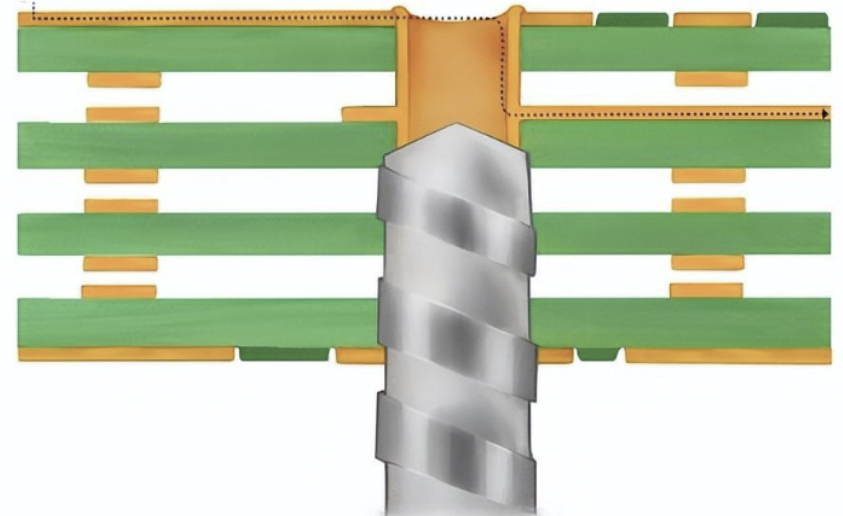 For low-speed signals, a via is merely an equivalent tiny parasitic capacitance and parasitic inductance; but for high-speed digital signals containing an extremely wide spectrum, the circuits inside the PCB have transformed into microwave transmission lines with distributed parameters.
A suspended via stub is equivalent to an open‑ended stub in a microwave circuit. When a high-speed signal enters the via, a portion of the energy will obediently travel along the target trace; but another portion of the energy will act as if it went astray, diving into this stub, rushing all the way to the bottom, and then generating a 100% total reflection due to the open circuit, bouncing back to the original path.
This reflected energy overlaps with the subsequent main signal. When the electrical length of this stub is exactly equal to one‑quarter of the signal’s wavelength, the signal has travelled back and forth, and the phase of the reflected signal will lag the main signal by exactly 180 degrees, creating perfect phase cancellation.
At this time, the stub, which is physically an open circuit, will exhibit short‑circuit characteristics at that specific frequency, forming a bottomless notch filter. This will swallow all the signal energy near that frequency, leading to severe signal attenuation, deterministic jitter, and eye diagram closure.
Practical Example: Assuming a stub length of 37 mil, in standard FR‑4 board material (dielectric constant ≈ 4.0), its resonant frequency falls around 30 GHz. This is a devastating blow to 25 Gbps or even higher speed signals. If the stub is shortened to 12 mil through backdrilling, the resonant frequency is pushed back beyond 80 GHz, posing no threat to current mainstream high‑speed signals.
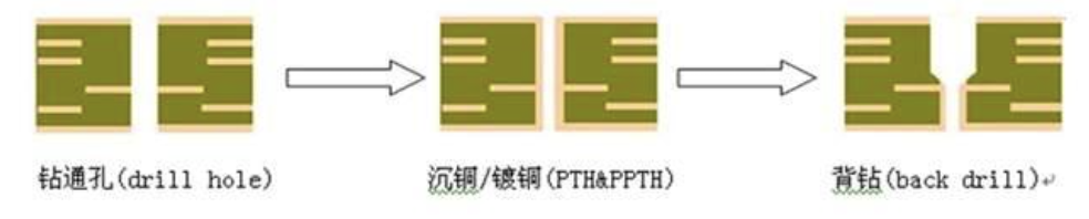
To eliminate this annoying stub, board factories must add a secondary drilling step to the standard PCB process – that is, using a slightly larger drill bit from the back of the board to clear out the excess copper tube at a specific point. The specific standard procedures are as follows:
From the perspective of a signal integrity engineer, a shorter stub is naturally better. If the residue can be shaved down to 0 mil, completely flush with the exit layer, that is the most perfect. But under realistic Design for Manufacturing considerations, this is impractical and extremely dangerous.
Backdrill equipment relies on calculating the distance from the board surface to the inner layer to control the drilling depth. However, after the PCB undergoes multiple high‑temperature laminations, the resin flow of the prepreg will cause fluctuations in board thickness, coupled with the board material’s own thickness tolerance (usually ±10%). If a 0 mil stub is forcefully demanded, as long as the machine presses down slightly deeper, it will directly drill through the copper ring and traces of the signal exit layer, scrapping the entire board directly.
 Therefore, “shallow is better than deep” is the iron rule of the backdrill process. To protect the exit layer, the board factory must reserve a safety distance. The following is the industry‑standard correspondence table between board thickness and backdrill residue length:
| Finished board thickness | Stub length (mil) | | :--- | :--- | | ≤ 1.6 mm | 2 – 8 | | 1.6 mm – 2.5 mm | 2 – 10 | | 2.5 mm – 3.8 mm | 2 – 12 | | 3.8 mm – 5.0 mm | 2 – 14 | | ≥ 5.0 mm | 2 – 16 |
Design note: These inevitable residual lengths must be factored into the front‑end signal simulation to ensure the system has enough margin to resist the minor degradation caused by the residual stub.
Aside from manufacturing tolerances, another fatal flaw often overlooked by engineers lies in the mechanical conflict between backdrill depth and press‑fit connectors.
On servers, backplanes, or large industrial control motherboards, high‑density connectors typically do not use surface mount soldering, but instead use a solderless press‑fit process. The metal pins of these connectors feature a hollow and elastic “eye‑of‑the‑needle” structure. When the pin is forcibly pressed into the PCB’s through‑hole, the eye is compressed and tightly grips the hole wall’s copper, thereby achieving electrical conduction and mechanical fixation.
Disaster Scenario: If you, in pursuit of ultimate high‑frequency performance, desperately request the board factory to drill the backdrill very deep, striving for the shortest stub, the result may be that the backdrill bit washes away a massive amount of hole copper, causing the remaining effective hole copper length to actually be shorter than the connector’s eye length.
When the connector is pressed in, the upper half of the eye is suspended in the insulated resin section washed away by the backdrill, unable to contact the hole copper at all. This not only causes an open signal circuit but also causes the connector to lose mechanical grip, loosening directly after a few insertion‑extraction cycles.
Golden Decision Sequence: When dealing with press‑fit holes, you must prioritise ensuring the integrity of the hole copper for the eye’s effective contact length, and only then pursue the shortest stub length. If the two conflict, you may even have to compromise and abandon backdrilling for specific layers, using other methods (such as switching to a board material with better dielectric constant and dissipation factor) to compensate for the loss of signal integrity.
Since via stubs are so troublesome, why not just completely switch to the High‑Density Interconnect (HDI) process? Using lasers to drill blind vias that only penetrate one or two layers would prevent stubs from being generated right from the start.
The answer is very realistic: cost and stack‑up limitations.
HDI requires multiple sequential laminations. For every added tier of blind vias, the board factory has to perform an additional cycle of lamination, drilling, and plating, causing costs to jump exponentially. For thick server boards that easily reach 16, 24, or more layers, quotes for full‑board blind and buried vias could be astronomical.
In contrast, the backdrill process only requires “drilling one more time” after the traditional mechanical through‑hole process, making the cost far lower than multiple laminations. Therefore, for products where routing density is acceptable but board thickness is extremely thick and signal rates are extremely high (such as core routers and AI computing motherboards), through‑holes paired with backdrilling are currently the most cost‑effective golden combination. However, it should be noted that the disadvantage of backdrilling is that it can only drill inward from the outer layers and cannot solve stub problems sandwiched in the middle layers of the board.
If you decide to enable the backdrill process in your product, please strictly adhere to the following three standard practices during the layout phase:
Anti‑pad clearances must be enlarged
The drill bit used for backdrilling is usually 0.15 – 0.2 mm (about 6 – 8 mil) larger than the original through‑hole diameter. Therefore, when setting design rules, the clearance between the trace and the inner copper plane around the via absolutely cannot be based on the original hole diameter; it must be expanded outward based on the backdrill hole diameter. An extreme safety clearance is recommended at 6 mil, and it is strongly recommended in regular design to maintain an anti‑pad distance of 10 mil or more to prevent slight drilling deviations during backdrilling from accidentally cutting adjacent high‑speed traces.
Prioritise optimising layer‑swapping strategies to eliminate backdrilling from the source
The best debugging is to not generate errors. If high‑speed signals enter from the top layer, try to plan the exit layer at the bottom layer or an inner layer close to the bottom. This way, the signal penetrates the entire board thickness, naturally leaving no long stub, and even the backdrill processing fee can be directly saved.
Clear drawing labels and drill charts
In the output manufacturing files or production instructions provided to the board factory, the drill pairs for backdrilling must be clearly defined. For example, labelling “Backdrill: Bottom Layer to Fifth Layer” clearly informs the factory engineers: this set of holes must be drilled from the bottom layer, and the depth must precisely stop before the fifth layer, absolutely without damaging the traces on the fourth layer.
The backdrill process is a sharp double‑edged sword. In layout software, shortening a stub is just a two‑click parameter setting; but on the actual factory floor, it involves the machine’s extreme tolerances, the cleanliness of high‑pressure washing, and even the assembly yield of terminal connectors.
Excellent hardware design is never a one‑sided pursuit of a theoretically perfect signal curve, but a precise game played among microwave electrical performance, mechanical structural strength, and large‑scale mass production costs. Understanding the backdrill limits of the factory and reserving reasonable tolerances and clearance spaces are the only ways to enable your high‑end design to truly achieve a first‑time pass and steadily advance toward mass production.
