May 4, 2026
In today's era of lightweight, thin, short, and small electronics, combined with high-speed and high-frequency requirements, the physical stability of Printed Circuit Boards (PCBs) has become a severe challenge for R&D engineers and packaging process experts. With the increase in component packaging density—especially the widespread application of Ball Grid Array (BGA) and Chip Scale Packaging (CSP)—even microscopic deformations in a PCB can lead to catastrophic manufacturing yield losses.
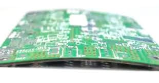
The phenomena of Bow and Twist—often vividly referred to in the industry as "potato-chipping"—are not only the culprits behind component throwing on Surface Mount Technology (SMT) lines but also the core root of BGA soldering failures, Head-in-Pillow (HiP) defects, and long-term reliability issues. This report deeply analyzes the causes and prevention of board warpage from four dimensions: physical mechanisms, technical pain points, Layout strategies, and manufacturing solutions.
To understand why PCBs deform, we must return to the essence of materials science. A PCB is essentially a heterogeneous composite material composed of Copper Foil, Resin, and Glass Cloth. These three materials exhibit vast differences in their thermal reactions when heated, and this disparity is the physical starting point of thermal stress.
The Coefficient of Thermal Expansion (CTE) is a key indicator measuring how a material expands or contracts with temperature changes. In a PCB structure:
Although expansion in the X and Y axes is typically restricted to a range close to copper foil due to the constraint of the glass fiber cloth, the uneven distribution of copper layers leads to completely asymmetrical tension and compression across different zones during heating or cooling.
When a PCB enters the high-temperature zone of a Reflow Oven, if the top layer has dense copper while the bottom layer is sparse, the top layer will have higher resistance to expansion (due to copper's low CTE), while the bottom substrate expands freely. This generates a downward bending moment. During cooling, the reverse occurs. This dynamic stress change eventually leads to permanent plastic deformation.
Copper Balance refers to the percentage of area covered by copper foil on each layer relative to the total layer area. In multi-layer design, if the Stack-up violates the principle of symmetry—for example, using Cores or Prepregs of different thicknesses on either side of the center layer, or having a massive difference in copper balance between two symmetrical layers—hidden dangers are planted during the Lamination process.
When these built-in stresses are partially released during subsequent drilling, etching, or baking processes, the board will exhibit visible bending. The table below presents a comparison of physical parameters for typical FR-4 material in different states, helping engineers understand why high temperature is the catalyst for deformation:
| Parameter Item | Unit | Copper Foil | FR-4 (Below Tg) | FR-4 (Above Tg) | | :--- | :--- | :--- | :--- | :--- | | CTE-Z | ppm/°C | 17 | 50-70 | 250-300 | | CTE-XY | ppm/°C | 17 | 12-16 | 12-16 | | Young's Modulus | GPa | 110-120 | 20-25 | < 5 | | Glass Transition (Tg) | °C | N/A | < Tg point | > Tg point |
From the Young's Modulus in the table, it is evident that when the temperature exceeds the Tg point, the rigidity of the substrate drops precipitously. This means its ability to resist stress hits rock bottom; if residual stress exists at this moment, the board is extremely prone to deformation.
On automated SMT production lines, PCB flatness is the foundation for ensuring precise placement of all components. IPC standards stipulate that PCB warpage for SMT placement should be ≤ 0.75%. However, in actual production for high-density BGA products, many manufacturers demand control within 0.5% or even 0.3%. When warpage exceeds specifications, a series of technical pain points ensue.

The working principle of an SMT pick-and-place machine involves picking up components via a vacuum nozzle and pressing them into solder paste based on coordinates defined by a visual recognition system. If board warpage occurs, the board surface is no longer a flat plane. The nozzle may press too deep in some locations (squeezing out solder paste and causing shorts) or not deep enough in others (causing poor contact between component and paste).
This leads to Component Throwing. When the machine detects incorrect component posture on the nozzle or fails to sense the expected resistance when pressing down to the preset height, the system judges it as a picking failure or placement anomaly, discarding the expensive chip into the waste bin. For extremely small components like 0201 or 01005, subtle PCB undulations (e.g., a 0.1mm height difference) are enough to disrupt placement accuracy, significantly increasing production costs.
Because BGA solder joints are hidden beneath the component, they have the strictest requirements for board flatness. Warpage can trigger two extreme phenomena on the same BGA:
This phenomenon of "Open at one end, Short at the other" is particularly common on large circuit boards (such as server motherboards). Additionally, the depth of V-Cut grooves significantly affects regional structural stress; overly deep V-Cuts can cause the board to fold at the groove under the clamping force of the reflow oven rails, further exacerbating deformation.
To completely solve the warpage problem, relying solely on process adjustments is often a temporary fix. Optimization of copper distribution by Layout engineers during the design phase is the golden rule for preventing deformation. The core goal is to achieve "Thermal Mass Balance" and "Structural Rigidity Symmetry" across all zones and layers of the board.

Designers should use the built-in functions of Electronic Design Automation (EDA) software to precisely calculate the copper balance of each layer. It is generally recommended to use the center layer of the PCB stack-up (e.g., between layers 3 and 4 of a 6-layer board) as the axis of symmetry, ensuring the copper balance difference between corresponding layers (e.g., L1 vs. L6, L2 vs. L5) is controlled within 10%.
When signal traces on a specific layer are very sparse, the copper rate might drop below 20%. In this case, "Thieving Copper" must be added to increase the copper content in that area. Thieving not only reduces current density differences during plating (avoiding uneven trace thickness) but also increases the thermal capacity of the board, reducing local temperature differentials during heating.
Using Cadence Allegro or Altium Designer as examples, Layout engineers can set automatic copper pouring rules:
Besides interlayer balance, the overall Stiffness of the PCB is closely related to the amount of deformation. According to the stiffness concept (proportional to Young's Modulus × Moment of Inertia), increasing the cross-sectional area or the elastic modulus can improve the ability to resist stress. In practice, increasing board thickness (e.g., from 1.0mm to 1.6mm) is the most effective method. However, if limited by product volume, the following reinforcements can be used:
The Fabrication end is the final line of defense for controlling warpage. As a professional PCB manufacturer, eCloud Technology has developed a manufacturing process based on stress relief for high-precision circuit boards, strictly adhering to international standards like IPC-6012.
PCB Lamination is a complex chemical process where Prepreg (PP) transitions from resin flow to curing. The "Cold Press Control" technology adopted by eCloud Technology emphasizes that after the hot press cycle ends, the pressure is not immediately released. Instead, the board enters a specialized cold press machine where the temperature is lowered at a precise slope (e.g., 1.5 to 2°C/min) while maintaining pressure. This allows resin molecules to rearrange uniformly while crossing the Tg point back to the glassy state, preventing massive thermal stresses from being "locked" inside the multi-layer structure.
For thinner boards (under 2.0mm) or complex boards with high layer counts, eCloud Technology performs a standardized "Baking Leveling" procedure before shipment. The PCBs are placed in an oven with heavy-weight fixtures and baked at a temperature slightly above the material's Tg for 4 to 6 hours. This forces the release of mechanical stresses accumulated during processes like drilling, etching, and plating.
According to IPC-TM-650 2.4.22B measurement specifications, eCloud Technology controls warpage for different product grades as follows:
| Product Type | Board Thickness (mm) | eCloud Tech Standard (Warpage %) | IPC-6012 Benchmark (%) | Note | | :--- | :--- | :--- | :--- | :--- | | General Telecom Board | 1.6 | ≤ 0.50% | ≤ 0.75% | Standard SMT | | Thin Wearable Device | 0.8 | ≤ 0.40% | ≤ 0.75% | High-difficulty control | | High-Speed Server | 2.4 | ≤ 0.30% | N/A (Custom) | For Large BGAs | | Single/Double Sided | 1.6 | ≤ 1.0% | ≤ 1.0% | Through-hole only |
To ensure every shipped PCB meets RD design expectations, eCloud Technology employs an Automated Optical Measurement (AOM) system. During measurement, the board is placed on a precision marble platform, and a laser rangefinder scans the full board for height differentials.
The calculation follows the industry standard formula:
Warpage% = (H/L)* 100%
Where H is the maximum height deviation and L is the length of the board's long edge or diagonal. For a panel with a diagonal length of 300mm, a 0.5% warpage means the height difference between the highest and lowest points must not exceed 1.5mm. This rigorous measurement standard is the key guarantee for zero defects in backend SMT placement.
For Mechatronics students and senior RDs, understanding warpage prevention is not just about "flatness"—it is a game between mechanical mechanics and electronic engineering. In actual design, stress relief measures sometimes conflict with electrical specifications.
This is a detail often overlooked by routing engineers: When we add large areas of Thieving on the Signal Layer to balance copper, this copper changes the fringe field distribution of transmission lines, leading to a drop in Characteristic Impedance.
For a 50 Ohm single-ended line, if the distance between the Thieving and the signal line is less than 2 times the line width (< 2W), the impedance may shift by 2 to 3 Ohms. In high-speed digital signals, this can trigger Reflection and Signal Integrity (SI) issues.
Deep Advice: When designing Thieving, set high-speed differential pair areas as "Keep-out" zones in the EDA software. Ensure Thieving maintains a distance of at least 5 times the line width (5W) from sensitive signal lines. This maintains mechanical balance without damaging electrical quality.
As AI computing chip power continues to climb, PCB operating temperatures are rising. Selecting materials with a Tg point higher than 170°C (e.g., IT-180A, S1000-2) has become standard. However, future technology trends are moving towards "CTE Matched Substrates", developing Low CTE CCLs that are closer to Silicon chips (CTE ≈ 2.6 ppm/°C) or ceramic packaging. This aims to eliminate structural stress caused by thermal cycling right at the material source.
Although board warpage is a century-old problem in the PCB industry, it is no longer an insurmountable challenge with the aid of modern simulation technology and precision craftsmanship. From an R&D perspective, warpage prevention begins with Copper Balance in the Layout phase; the ingenious application of Thieving injects stable structural genes into the PCB. On the manufacturing side, choosing a partner like eCloud Technology—possessing deep process capabilities, strict adherence to IPC-6012 standards, and cold press controls—is critical to ensuring designs are translated into high-quality physical products.
For every frontline RD and Mechatronics engineer, mastering this DFM knowledge system—spanning from physical fundamentals to practical Layout and manufacturing verification—is not just about improving production yields. It is about crafting a truly robust and flat "electronic heart" in this high-speed era where "a miss is as good as a mile."
