May 9, 2026
For RD and PCB Layout engineers fighting on the front lines, designing a stackup often involves a tug-of-war between "impedance control," "board thickness," and "manufacturing cost." When negotiating with PCB fabrication houses, you might have heard them suggest a special structure called a "fake 8-layer board" (or dummy 8-layer board). If the schematic only calls for a 6-layer routing plan, why upgrade to an 8-layer structure? Is this a waste of budget, or does it hide some manufacturing ingenuity? Today, we will thoroughly analyze this special multi-layer board design structure.
In the PCB industry, we usually define the number of layers by the "number of copper foil routing layers." A standard 8‑layer board stackup usually consists of 3 core boards (Cores), 4 layers of prepreg (PP), and top and bottom outer copper foils pressed together, resulting in a total of 8 copper layers with routing.
 A "fake 8‑layer board" , however, is essentially a 6‑layer board. Its approach is to adopt the physical stackup structure of an 8‑layer board, but the copper foil on the top and bottom of the middle Core (which corresponds to L4 and L5 in a standard 8‑layer board) is completely etched away, turning it into a "bare board / Dummy Core" without any routing.
This means that although the board is stuffed with 3 Cores and has the thickness and lamination structure of an 8‑layer board, it actually only has 6 copper layers with conductive functions.
Note: Occasionally, there is another situation where, for cost or special design reasons, 2 layers of copper foil plus PP are used to replace the middle Core. Although it retains 8 copper layers, it changes the standard lamination structure. This is also sometimes broadly referred to as a fake 8‑layer in the industry, but today we are primarily discussing the former, most common situation.
The answer is simple: to meet the dual requirements of "board thickness" and "impedance control."
When we design a 6‑layer board with a thickness of 1.6 mm (or more), if strict impedance control is required (e.g., single‑ended 50 Ω, differential 100 Ω), the trace width and dielectric thickness must be precisely matched. After adjusting these parameters, it often causes the spacing between the middle layers (i.e., between L3 and L4) to become very large.
This excessively large spacing poses severe challenges during manufacturing.
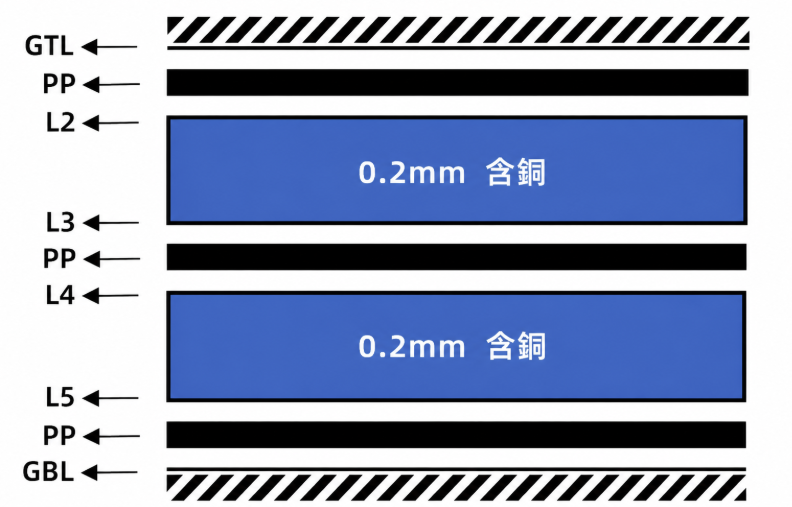
To fill the thicker dielectric layer between L3 and L4, the intuitive approach is to stack multiple layers of PP (such as 7628). However, from the perspective of the PCB manufacturer's process, this is a hidden landmine.
During the high‑temperature PCB lamination process, the PP transitions from a semi‑cured state to a liquid resin and flows. The industry‑recognized safety limit is: a maximum of 3 sheets of PP can be stacked. Once it exceeds 3 sheets, the liquid resin easily overflows excessively from the edges of the panel, leading to uneven board thickness, interlayer slippage, and even serious reliability issues (such as delamination or board bursting).
This is where the Dummy Core of the "fake 8‑layer board" comes in handy! Rather than risking stacking 4 or more sheets of PP, it is better to insert an already cured "copperless Core (bare board)" directly between L3 and L4. This not only perfectly makes up the required dielectric thickness and precisely meets the impedance requirements, but also maintains the stability of the lamination process and ensures the yield rate.
The design logic of the "fake 8‑layer" can also be applied to a "fake 6‑layer board." As an engineer, when faced with such stackup choices, you can evaluate the following points:
The fake 8‑layer board is not a gimmick for manufacturers to earn more material fees, but a product of wisdom compromised between PCB manufacturing processes and high‑frequency impedance design. Next time you receive a Stackup proposal from a board house, you will undoubtedly understand the considerations behind it immediately!
