August 12, 2026
As AI servers, mobile motherboards, silicon photonics, and edge-computing devices keep pushing toward higher density, engineers who cut their teeth on the four- and six-layer through-hole boards behind TVs and home appliances hit an unfamiliar term the moment they touch mobile-class products: the HDI board. Worse, HDI itself splits into HDI1, HDI2, HDI3, all the way up to ELIC any-layer. For the same 8-layer board, moving between grades can swing the quote by two to three times and stretch lead time from half a month to well over a month. In this article, we start from the manufacturing-side physics and lay out — in one pass — what the HDI stackup grades mean, the key via processes behind them, and the cost and lead-time logic that follows.
The fundamental reason HDI exists is that a mechanical drilled hole simply won't fit.
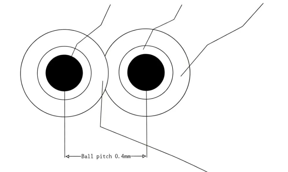
Chips in VFBGA packages have very fine pad pitch. Take 0.4 mm pitch: drill a 0.3 mm mechanical through‑hole and, once you add the annular ring on each side, the outer diameter reaches about 0.5 mm — but the solder balls sit only 0.4 mm apart. Since 0.5 mm > 0.4 mm, the hole doesn't fit, and adjacent vias interfere or even short.
A laser microvia changes the picture entirely: a 0.1 mm laser hole with its annular ring measures about 0.22 mm across, and can land directly on the chip's 0.25 mm pad. That leaves 0.4 mm of clearance between vias — equal to the ball pitch — with no interference at all.
Here's a practical rule of thumb: a 0.65 mm ball‑pitch BGA has room for a 0.3/0.5 mm mechanical via between balls, so it doesn't need HDI. Once pitch tightens to the 0.4 mm class, fanout has to rely on laser microvias — which means HDI becomes unavoidable.
Before you can read an HDI stackup drawing, you need to separate "types of vias" from "ways of stacking vias."
The first set is drill depth:
On an 8‑layer HDI2, for example, Via 1–3 is blind, Via 3–6 is buried, and Via 1–8 is a through via.
The second set is how adjacent microvias stack — stacked vs. staggered:
| Comparison | Stacked Via | Staggered Via | | :--- | :--- | :--- | | Position | Concentric and vertically aligned, forming a copper pillar | Laterally offset, not overlapping | | Process | Lower via must be copper‑filled and planarised before the upper one is stacked | Lower via only needs barrel plating | | Difficulty & cost | High (multiple fill‑plating cycles) | Low | | Signal & routing | Shortest path, better SI/PI | Requires a short L2 inner‑layer trace to connect |
In practice, HDI laser vias are mostly stacked, because they save space, shorten routing, and are more favourable for signal quality and power integrity.
"Grade" refers to how many build‑up cycles and laser‑drilling rounds are done on a single outer side.
The standard notation reads 1+N+1, 2+N+2, 3+N+3, where the middle N is the number of inner layers in the core, typically interconnected by conventional mechanical through‑holes or buried vias. The difference between grades comes down to how many layers a blind via can span and whether it can be stacked:
| Grade | Standard Stackup | Build‑up / Laser Rounds (per side) | Stacked Via? | Surface Reaches | | :--- | :--- | :--- | :--- | :--- | | HDI1 | 1+N+1 (e.g. 6‑layer 1+4+1) | 1 | No, adjacent‑layer blind only | L2 | | HDI2 | 2+N+2 (e.g. 8‑layer 2+4+2) | 2 | Stacked / staggered supported | L3 | | HDI3 | 3+N+3 (e.g. 10‑layer 3+4+3) | 3 | Continuous three‑layer stepped blind | L4 |
HDI1 is the simplest: blind vias connect only adjacent layers, cannot cross layers (no L1 straight to L3), and stacking is not allowed. With HDI2, the surface can jump directly to the third layer, and both stacked and staggered vias are supported. HDI3 can build continuous stepped blind vias — L1→L2→L3→L4 — with the surface reaching the fourth layer directly. Every added grade means another independent round of build‑up and laser processing, and cost and lead time climb accordingly.
ELIC (Every Layer Interconnect) is HDI's top‑tier process — a laser microvia can be drilled between any two adjacent layers.
In conventional 2‑ and 3‑stage HDI, a solid core sits in the middle; inside that core you can only place mechanical buried vias, because a laser via can't cross it. ELIC has no thick core (note carefully — no thick core, not zero core). The whole board is stacked from thin build‑up layers, so any layer can interconnect with any adjacent layer, and both routing and cross‑layer paths reach their shortest form. Because it isn't bound by a fixed number of outer build‑up cycles and can stack microvias freely on every layer, ELIC offers far more routing freedom than a fixed 3+N+3 HDI3. As for a full‑board connection like Via 1–10 on a 10‑layer any‑layer board, it's still executed with stacked laser vias in practice — even though a mechanical hole would be cheaper, the process generally won't introduce one just for that.
If you want ELIC, the first thing to check isn't layer count — it's board thickness.
ELIC's premise is that every layer can be laser‑drilled. Once a board gets too thick (say 1.6 mm), an overly thick core appears in the middle that the laser can't penetrate, forcing a return to mechanical drilling. On a 10‑layer board, if the core is too thick to laser, the best you can do is HDI4, with that middle section still interconnected by mechanical drilling — it looks like any‑layer, but because of those mechanical holes it's fundamentally still HDI4.
This also clears up a common misconception: a board with blind and buried vias isn't necessarily HDI. The key is whether the blind via is a laser microvia or a mechanical hole. If it's mechanical, it's still just an ordinary multilayer board.
Higher isn't better — just‑enough is cheapest.
As a rough production‑experience estimate: HDI3 typically runs 30%+ more than HDI2, and ELIC more than doubles HDI2. Lead times have no fixed value, but you can anchor on experience:
| Stackup Grade | Relative Cost | Typical Lead Time | | :--- | :--- | :--- | | HDI2 (2+N+2) | Baseline | ~15 days | | HDI3 (3+N+3) | 30%+ more | ~25 days | | ELIC any‑layer | More than double | ~35 days |
This latest wave of AI hasn't just pushed memory prices up — PCBs have surged along with it, making stackup choices more cost‑sensitive than ever. The most common waste we see in practice is forcing a design that 1+N+1 could handle into 2+N+2, or piling on stacked vias where none are needed. The extra money rarely buys matching performance.
From the physical limits of VFBGA fanout, through stacked and staggered vias and blind/buried/through vias, up from HDI1 all the way to ELIC — every grade of HDI stackup is another layer of build‑up and laser processing stacked on, and another jump in cost and lead time. Real engineering skill isn't in drawing the board as high‑grade as possible; it's in using a just‑enough stackup to drive cost and yield risk as low as they'll go.
eCloud provides integrated services from prototype to complex HDI/ELIC builds, with deep experience across high‑speed networking, silicon photonics, edge AI, and RF/high‑frequency applications. Planning the stackup for your next HDI project? Reach out to our engineering team at the layout stage to get an early DFM pre‑review — pick the right grade and bring both cost and yield risk down together.