August 16, 2026
As high-speed digital, automotive electronics, and high-density packaging keep advancing, copper pour is often treated as a "fill the gaps" afterthought at the end of layout. But from a manufacturing standpoint, copper pour has never been merely cosmetic. It shapes signal return paths, thermal performance, and EMI behavior — and it directly drives inner-layer copper coverage, lamination quality, and final board thickness. This article unpacks the engineering logic behind copper pour, from design to fabrication.
At its core, copper pour fills the unused regions of a PCB's copper layers with large copper areas (solid or hatched) tied to a power or ground net, forming a continuous conductive plane. It plays three roles at once:
Beyond these, a stable reference plane improves the waveform integrity of high‑speed signals, and sensible pour can reduce extra routing — indirectly saving copper and cost. In short, copper pour is a design lever that delivers multiple benefits from a single action.
The most overlooked copper‑pour detail — and the one that most often bites you on the line — is how a pad connects to the pour. Copper's thermal conductivity is high, around 380 W/(m·K). If a pad is fully connected to a large copper area on all sides, heat is wicked away rapidly during reflow or hand soldering, causing poor wetting, cold joints, and dry joints.
Thermal relief pads solve this by connecting the pad to the pour with a few thin spokes, deliberately raising local thermal resistance so heat stays near the joint and solderability is preserved. In practice, pads needing high current or active heat‑sinking can keep a full connection, but general signal and passive‑component pads should use thermal relief as a default.
Copper pour comes in two styles — solid and hatched — and choosing the wrong one can, in the worst case, keep a circuit from working. Solid pour offers the best current capacity and shielding, but large copper areas are prone to warping and copper lifting under wave soldering; the common fix is to design slots/openings into the pour to relieve stress. Hatched pour uses less copper, dissipates heat better, and still shields, but carries less current — and, critically, when the length of the hatched copper "segments" approaches the electrical length of the operating frequency, those segments behave like an array of small antennas radiating interference, which can render the circuit inoperable.
| Criterion | Solid | Hatched | | :--- | :--- | :--- | | Current capacity | High | Low | | Shielding | Strong | Adequate | | Heat dissipation | Weaker (more copper) | Better (less copper) | | Wave‑solder warping risk | High (needs slots) | Low | | High‑frequency EMI | Stable | Worse if segment length is off |
A process reality worth noting: fabs have broadly moved from low‑cost wet film to the superior dry film process, and hatched pour tends to crack dry film at the fine gaps. So in most cases, prefer solid; reserve hatched for high‑frequency designs with explicit EMI needs, and use solid for low‑frequency or high‑current circuits.
In high‑frequency circuits, a poorly grounded copper pour is more dangerous than no pour at all. At high frequency the distributed capacitance of traces comes into play; once a trace exceeds 1/20 of the wavelength (λ/20) of the noise frequency, it radiates that noise into the surrounding space like an antenna — and any poorly grounded pour helps propagate it.
That's why high‑frequency grounding needs more than electrical continuity: ground‑tie spacing must stay below λ/20. The practical method is to stitch ground vias along the pour so it's truly connected to the ground plane of the multilayer board — improving current capacity and lowering EMI at the same time, instead of letting a sheet of copper become a "false ground" antenna array.
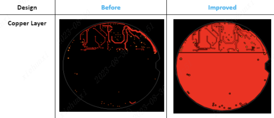
If you take one thing from this article, take this: insufficient inner‑layer copper changes board thickness and lamination yield where you can't see it. Copper coverage is the ratio of remaining copper area to total board area on an inner layer after etching.
During lamination, prepreg (PP) is placed between cores; under heat and pressure the resin flows to fill regions with no copper on adjacent layers and bonds the stack together. When an inner layer's copper coverage is too low, the resin has to flow farther to fill the gap — resulting in thinner‑than‑expected boards, wrinkles in copper layers, resin voids, or even delamination from resin starvation. The design‑side compensation is straightforward: add pour to empty regions where possible, and keep at least 0.5 mm clearance from high‑speed traces to balance copper coverage against signal quality.
Copper coverage isn't abstract — it feeds directly into the fab's thickness math. Cured PP thickness isn't fixed; it is:
Cured PP thickness = Uncured PP thickness − ((1 − copper coverage) × copper thickness)
For an example L1/L2 stackup: uncured PP of 4.72 mil, L2 copper coverage of 85%, and 1 oz inner copper gives cured PP = 4.72 − ((1 − 85%) × 1.2) = 4.54 mil. (Note: 1 oz is nominally 35 μm, but after pre‑processing and browning losses the actual thickness is about 30 μm, i.e. 1.2 mil.)
Summing the layers:
In one line: every shift in copper coverage moves the cured PP thickness, and the board thickness with it — which is exactly why "copper pour" feeds back into "stackup."
The final round of copper pour happens after you hand off the Gerbers — on the manufacturing side. In eCloud's fabrication flow, we add copper pour to the handling rails, bridge pieces, and other areas outside the PCB units on the panel, to prevent low board thickness and uneven plating caused by large empty spaces. This added copper sits only outside the PCB units and never touches anything inside the customer's board; we also leave the necessary clearance around fiducials, mechanical holes, mouse bites, and V‑cuts so downstream processing isn't affected. It's a textbook case of "the design side does its part, and the fab adds one more."
Copper pour looks basic, yet it spans signal integrity, thermal management, EMI, copper‑coverage balance, and thickness control. Prefer solid pour, use thermal relief well, stitch solid grounding on high‑frequency pours, and keep inner layers adequately covered with 0.5 mm clearance from high‑speed traces — these calls, made at the prototype stage, largely determine a board's final yield and consistency.
eCloud provides integrated fabrication from prototype to multilayer and HDI boards, and specialises in stepping in at the layout stage on copper‑coverage balance, stackup planning, and signal‑integrity DFM review. Still working out the stackup and pour strategy for your next project? Talk to our engineering team early and cut board‑thickness and lamination‑yield risk before it's designed in.
