February 1, 2026
As semiconductor process technology advances to the nanometer level, Moore's Law has not only driven the exponential growth of transistor density within chips but also imposed strict miniaturization requirements on Backend Packaging technology. In the fields of mobile devices, wearable electronics, IoT, and High-Performance Computing (HPC), chip packaging has shifted entirely from traditional Quad Flat Packages (QFP) to Ball Grid Array (BGA) and Wafer Level Chip Scale Packages (WLCSP). Among these, the W8-4BGA (0.4mm Pitch BGA), representing high-density packaging, has reached an extreme I/O pitch that is becoming a critical bottleneck for current hardware design and PCB manufacturing processes. For R&D engineers, hardware engineers, and electromechanical students, the traditional "Dog-bone" fanout strategy has been rendered ineffective by physical spatial limitations when facing the 0.4mm pitch challenge. The design paradigm must shift toward High-Density Interconnect (HDI) technology, specifically Via-in-Pad (VIP) and its core process: Plated Over Filled Via (POFV). However, this technical transition is not merely a change in routing; it involves drastic changes ranging from PCB stack-up design and material selection to process yield control and final production costs. This report aims to provide a detailed technical guide, deeply analyzing the inevitability of the transition from standard fanout to VIP processes. The report will explore the physical mechanisms of the POFV process, explaining why resin plugging and planarization are mandatory to avoid solder bubbles and Solder Wicking. Simultaneously, addressing the cost sensitivity of both academia and industry, it provides a detailed cost structure analysis and decision model comparing standard vias against VIP processes. Finally, this report calls for high-precision design consultation for high-density projects to ensure the best balance between performance, reliability, and cost.
The trend of electronic products being "light, thin, short, and small" has been the most significant feature of the electronics industry over the past thirty years. This drive comes primarily from consumer demand for portability in mobile devices (smartphones, tablets) and the extreme volume requirements of wearable devices (smartwatches, TWS earbuds). To accommodate more functional chips within a limited PCB area, packaging technology must continuously shrink the I/O Pitch.
In the 1990s, the emergence of BGA packaging solved the issues of easily bent pins and limited density associated with QFP. Early BGA ball pitches were concentrated around 1.27mm and 1.0mm, which was relatively spacious for PCB processes at the time. However, as I/O counts increased and package sizes shrank, the pitch rapidly decreased to 0.8mm and 0.65mm. Entering the 2010s, with the maturity of WLCSP (Wafer Level Chip Scale Package) technology, 0.5mm and 0.4mm pitches became mainstream for high-end consumer electronics, with 0.35mm pitch products even beginning to enter mass production.
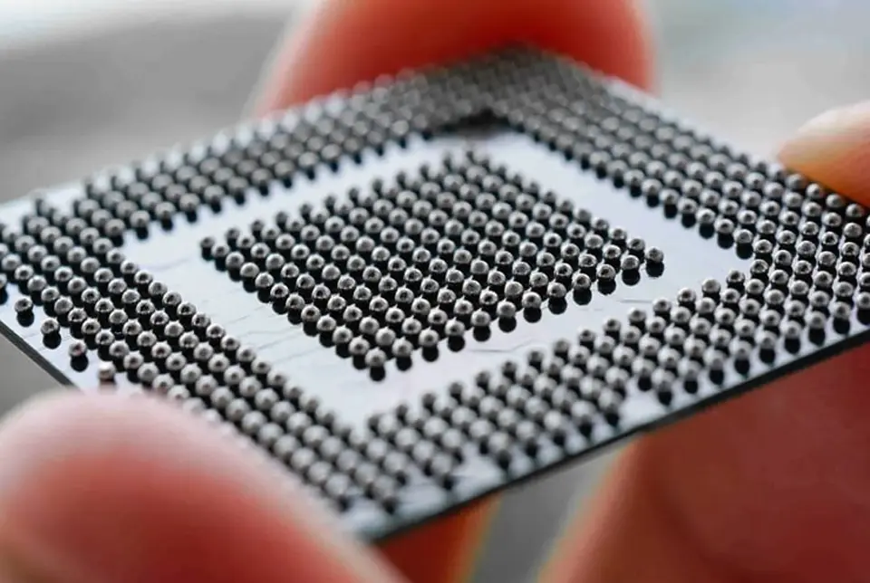
Components like the W8-4BGA (0.4mm Pitch) represent a critical point in current PCB design and manufacturing. At this spacing, PCB Routing Density faces geometric challenges. Every reduction in pitch is not just a change in numbers, but a comprehensive test of material science, mechanical drilling precision, optical alignment systems, and chemical plating capabilities.
In PCB design, the classic and lowest-cost BGA fanout method is called "Dog-bone" fanout. This structure consists of three parts: the BGA Pad, a short Trace, and a Via. From a top-down view, it resembles a dog bone. For BGAs with a pitch of 0.8mm or larger, dog-bone fanout is the standard solution, allowing signals to route from the pad to the via, and then through the via to inner or bottom layers.

However, when we switch the scenario to 0.4mm Pitch, geometric mathematical calculations declare the "death" of dog-bone fanout. We demonstrate this through specific dimensional analysis:
 . Obviously, a 0.35mm via pad cannot fit into a 0.2mm gap.
 (approx. 2.5mil). This approaches the process limit of many PCB factories and is highly prone to short circuits due to etching tolerances.
Conclusion: Data shows that when Pitch is less than 0.5mm, the space required for traditional mechanical drilling dog-bone fanout exceeds physical limitations. Although technically possible using extremely expensive high-end HDI processes with micro laser vias to force a similar structure, based on yield and cost considerations, the design paradigm must shift: from "Planar Bypass Fanout" to "Vertical Fanout," which is the Via-in-Pad technology.
The IPC-7351 standard defines general requirements for surface mount design and land pattern styles. For 0.4mm Pitch BGA, the pad design suggested by IPC is typically NSMD (Non-Solder Mask Defined).
Under the 0.4mm Pitch NSMD design, the copper pad is extremely small and independent. Attempting to route a trace from this tiny copper pad to an external via not only occupies valuable routing channels but also increases the risk of shorts with adjacent pads due to etching errors. In contrast, drilling directly in the center of the pad (VIP) completely eliminates the need for horizontal routing, guiding the signal directly to the inner layers. This is the only viable 0.4mm Pitch solution that complies with IPC standards. VIP technology allows designers to achieve high-density fanout without violating DRC (Design Rule Check).
Via-in-Pad (VIP) places the via directly within the pad of the Surface Mount Device (SMD). For high-density packages like W8-4BGA, VIP technology is not only a savior for freeing up routing space but also brings significant improvements in electrical and thermal performance.
VIP eliminates the short trace (Stub) and independent via footprint found in dog-bone structures. This means PCB surface space utilization is significantly improved; areas originally used for fanout can now be used for routing or placing decoupling capacitors. For 0.4mm Pitch BGA, this is almost the only choice as it does not require reserving via space between pads.
In high-frequency, high-speed circuits, every excess segment of wire (Stub) acts as an antenna or parasitic inductor/capacitor. Although the short trace in a dog-bone structure is small, at GHz-level frequencies, it still introduces considerable Parasitic Inductance and capacitive effects, causing signal reflection and attenuation. VIP guides the signal vertically from the solder joint to the inner layer via the shortest path, minimizing parasitic parameters and significantly optimizing high-speed signal transmission quality.
For high-power chips, heat dissipation is a core issue. In traditional designs, heat must conduct through the pad to the PCB surface and then spread horizontally. VIP design places the via directly under the heat source (chip solder joint), creating a vertical heat dissipation channel from the chip straight to the inner Ground Plane or bottom layer. The high thermal conductivity of copper makes VIP an excellent micro thermal pillar, significantly reducing the chip's Junction Temperature.
Although VIP has many advantages, drilling directly on the pad without post-processing will cause serious assembly issues. Therefore, VIP must be used in conjunction with the POFV (Plated Over Filled Via, also known as VIPPO) process.
POFV refers to filling the via with resin, curing it, grinding it flat, and finally plating a layer of copper (Cap Plating) on the surface to restore it to a complete, flat pad in both appearance and function. It is the process of turning a "Hole" back into a "Pad."
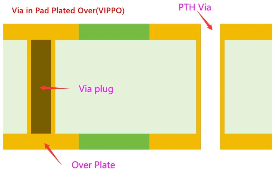
POFV Standard Process Flow:
For RD students and engineers, understanding "why we spend extra money on POFV" is crucial. If the POFV step is omitted and solder paste is applied directly to an open drilled pad (so-called "Via-in-Pad open"), it leads to two core defects that are physically unacceptable:
This is the most intuitive and destructive physical phenomenon. When the BGA solder ball is heated to its melting point (approx. 217°C - 245°C) in the Reflow oven, the solid solder ball turns into liquid. Liquid solder has high fluidity and surface tension.
Even if solder doesn't completely drain away, unfilled or poorly filled vias trap air inside. In the high-temperature environment of reflow, the behavior of these gases follows the Ideal Gas Law  , causing volume and pressure to increase drastically.
BGA components have extremely high requirements for PCB pad coplanarity. If the resin bumps up or dimples too much after plugging, BGA soldering will fail.
Therefore, the "Grinding" and "Copper Reduction" steps in POFV are key to ensuring Flatness. This is a detail low-end PCB shops struggle to control and is a core competency of high-end HDI shops.
In school labs or startup R&D environments, designers often prioritize Functionality. However, in Mass Production, Cost is the key to product survival. Introducing VIP and POFV significantly changes the PCB cost structure, a commercial sensitivity every engineer must possess.
The cost difference between standard Through-Hole and VIP/POFV is not just material cost, but the superposition of process complexity and yield risk.
For RD students and engineers, we establish a relative cost model, using a standard 4-layer board without VIP as the baseline (Index = 1.0):
| Feature Comparison | Standard Via | Via-in-Pad (VIP) + POFV | Cost Difference & Reason | | :--- | :--- | :--- | :--- | | Applicable BGA Pitch | > 0.65 mm | ≤ 0.5 mm (Essential for W8-4BGA) | Fundamental difference due to tech barrier; no substitute. | | Drilling Process | Mechanical Drill, 1 pass | Mechanical/Laser Drill + Multi-pass potential | POFV increases registration difficulty; Laser is costlier. | | Plating Process | 1 Plating Cycle | 2 Plating Cycles (Hole + Cap) | Increases plating time, chemical cost, and waste treatment. | | Filling Material | Solder Mask or None | Specialized Epoxy Resin | Resin is expensive and requires vacuum equipment. | | Surface Finish | HASL / ENIG | Must be ENIG or OSP | HASL is too uneven for fine pitch VIP; ENIG costs more. | | Bare Board Cost | Baseline (100%) | Increases 15% - 30% | Derived from added steps, capacity usage, and yield loss. | | Lead Time | Standard (3-5 Days) | Extended 1-3 Days | Waiting for long resin curing cycles and extra plating. |
Cost Insights for Engineers: Although VIP increases the bare PCB unit price by about 20%, in high-density designs, it may actually lower the total system cost. This is a counter-intuitive but important concept:
When designing with VIP, Taiwanese engineers cannot rely on verbal descriptions. You must be familiar with IPC (Association Connecting Electronics Industries) standards to accurately define requirements.
Taiwan possesses the world's most complete and advanced PCB and Substrate supply chain. Major players like eCloudPCB (eCloud Technology), Unimicron, Nan Ya, Compeq, and Kinsus have mature capabilities in HDI, Any-layer, and SLP processes for handling 0.4mm or even finer pitches (e.g., 0.3mm WLCSP).
Specific Call to Action for Taiwanese RDs, Engineers, and Students:
The emergence of W8-4BGA (0.4mm Pitch) marks a watershed moment in PCB design. At this extreme spacing, traditional "Dog-bone" routing logic is constrained by physical space and is no longer applicable. Via-in-Pad (VIP) paired with POFV (Resin Plugging and Cap Plating) has become the only reliable physical implementation path.
Although the POFV process introduces complex steps like resin filling, vacuum degassing, planarization, and secondary plating--raising bare board costs by 15%-30%--it solves fatal Solder Wicking and Voiding issues, ensuring soldering yield, electrical performance, and thermal efficiency for high-density packages. From a Total Cost of Ownership perspective, by reducing layer counts, minimizing size, and improving yields, VIP is often the more economic choice.
We call upon Taiwanese R&D teams and future engineers to actively adopt design rules compliant with IPC-4761 Type VII when facing such high-density designs, leverage Taiwan's powerful PCB supply chain resources, and actively seek professional technical consultation. Only by deeply understanding the trade-offs between process details, physical mechanisms, and cost structures can you design excellent products that are advanced, reliable, and competitive in mass production within the fierce global hardware race.
| English Term | Chinese Term | Brief Explanation | | :--- | :--- | :--- | | Via-in-Pad (VIP) | 盤中孔 | Technology placing the via inside the component pad for high-density routing. | | POFV / VIPPO | 樹脂塞孔電鍍填平 | Plated Over Filled Via. Standard VIP process including resin filling, grinding, and cap plating. | | Dog-bone Fanout | 狗骨頭扇出 | Traditional BGA fanout using a short trace to connect pad and via. | | Pitch | 間距 | Distance between center points of BGA balls. 0.4mm is the high-density divide. | | Solder Wicking | 滲錫 / 錫膏陷落 | Liquid solder flowing into an open via due to capillary action, causing open joints. | | Planarization | 平整化 | Mechanical grinding to remove excess resin/copper after plugging to ensure flatness. | | Dimple | 凹陷 | Tiny depression left on the surface after resin plugging; must meet IPC-6012 (usually <2mil). | | HDI | 高密度互連 | High Density Interconnect. PCB tech using Microvias, fine lines, and blind/buried vias. | | IPC-4761 Type VII | IPC Type VII 規範 | Refers to "Filled and Capped Vias," the standard for protected vias. |
(This report is compiled based on IPC standards, PCB manufacturer technical manuals, TI packaging specifications, and practical experience from the electronic engineering community.)
