If you're like I was years ago when I first graduated—unfamiliar with this field and wanting to learn more about the basic concepts of impedance in PCB manufacturing—please continue reading. We'll guide you through understanding this important concept.
What is Impedance?
In circuits, the concept of "impedance," explained in simpler terms, refers to the combined effect of capacitance, resistance, and inductance generated in a conductor during AC signal transmission. This occurs due to alternating current variations according to electromagnetic induction principles. Collectively, this is called "impedance."
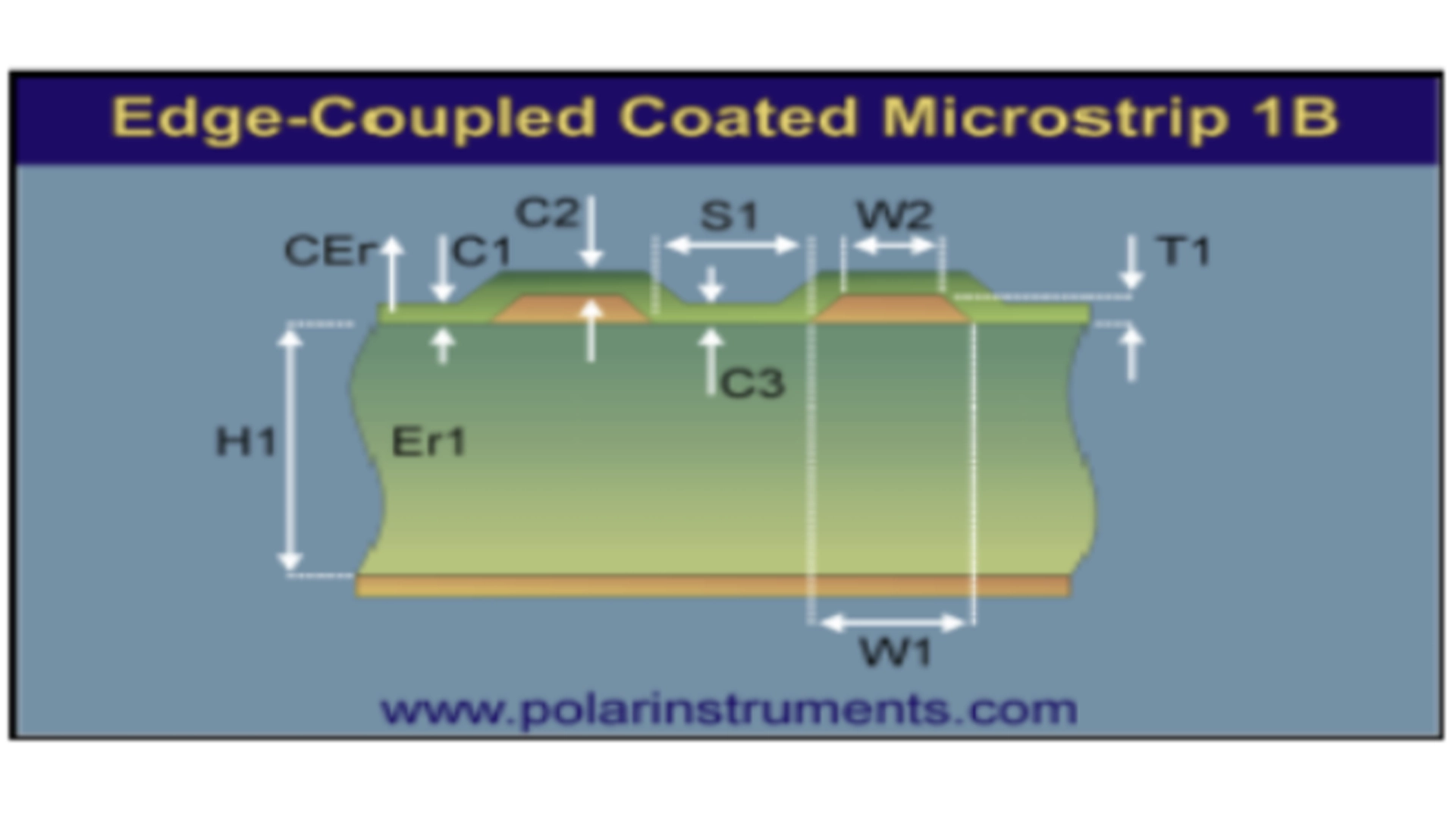
Outer layer:
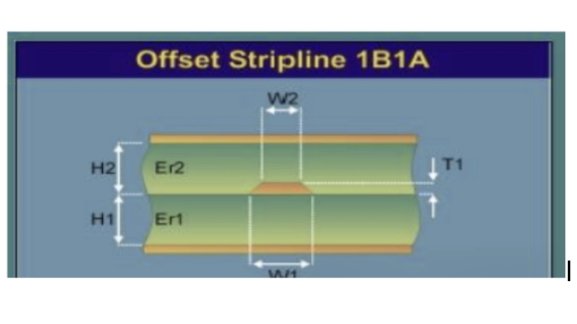
Inner layer::
Precise Definition of Impedance
In circuit analysis, Impedance (Z) is a comprehensive concept. Think of it as an extension of "resistance" in the AC (Alternating Current) world. It represents the overall "obstructive effect" that a circuit segment or component exerts on AC signal transmission.
Two Components of Impedance
This "total obstruction" consists of two parts:
1. Resistance (R)
- It represents energy-dissipative obstruction to current.
- Regardless of how current direction changes, it consumes electrical energy and converts it into heat.
- This is a real number.
2. Reactance (X)
- It represents energy-storing/inertial obstruction caused by capacitance (C) and inductance (L).
- They don't consume energy but periodically store and release energy, thereby "resisting" changing currents.
- This is an imaginary number.
Two Forms of Reactance:
- Capacitive Reactance (Xc): Generated by capacitance. The higher the frequency (f), the smaller the capacitive reactance.
- Calculation formula:
Xc = 1 / (2 * π * f * C)
- Inductive Reactance (XL): Generated by inductance. The higher the frequency (f), the larger the inductive reactance.
- Calculation formula:
XL = 2 * π * f * L
Mathematical Expression of Impedance
Therefore, the complete mathematical expression of impedance is a complex number:
Z = R + jX
Where:
- Z is impedance (unit: Ohm, Ω)
- R is resistance (real part, unit: Ohm, Ω)
- X is reactance (imaginary part, unit: Ohm, Ω)
- j is the imaginary unit (√-1)
Characteristic Impedance in PCB Design
In the PCB field, the impedance we discuss typically refers specifically to Characteristic Impedance and related impedance types.
Main Impedance Types
- Single-ended (Line) Impedance: The characteristic impedance value of a single signal trace.
- Differential Impedance: The characteristic impedance value measured between two transmission lines of equal width and spacing during differential driving.
- Coplanar Impedance: The characteristic impedance value measured when a signal trace transmits between surrounding GND/VCC (with equal spacing from the signal trace to GND/VCC on both sides).
- Insertion Loss: The energy attenuation from the signal source through the signal trace (channel) from the transmitter to the receiver.
- Single-ended loss is represented by the S21 symbol
- Differential loss is represented by SDD21
Nature of Characteristic Impedance
- It is not the impedance of a lumped element (like a resistor or capacitor's impedance).
- It is a distributed property of the transmission line itself (such as microstrip lines or striplines on a PCB).
You can think of it as the instantaneous resistance that a signal "feels" at each step as it propagates along a transmission line. Its value is determined jointly by the transmission line's physical structure and materials:
- Parasitic Resistance: From the copper foil of the conductor
- Parasitic Inductance: From current flowing through the conductor itself
- Parasitic Capacitance: From the electric field between the signal trace and adjacent reference planes (ground or power)
The characteristic impedance of an ideal transmission line is a real number (e.g., 50 Ω), which is a pure resistance. This means that at high frequencies, signal energy propagates along the transmission line without reflection (provided impedance matching), as if being absorbed by a resistor.
Single-ended Impedance vs. Differential Impedance
The distinction between these two modes is also correct; they are the two core concepts in high-speed PCB design.
1. Single-ended Impedance
- Definition: The impedance between a signal trace and its reference plane (usually the ground plane).
- Signal Mode: Signal voltage is measured relative to a fixed reference ground plane.
- Key Influencing Factors: Line width (W), spacing (S), dielectric thickness (H), copper thickness (T), substrate dielectric constant (Er), solder mask thickness, etc.
- Common Values: 50 Ω (e.g., USB, SD cards, most RF lines).
- Advantages: Simple routing, space-saving.
- Application Scenarios: Ordinary low-speed signals, clock signals, RF signals.
2. Differential Impedance
- Definition: The impedance between a pair of differential signal traces with opposite phases.
- Signal Mode: The signal is the voltage difference between two traces. One trace carries the positive signal (+), the other carries the negative signal (-).
- Key Influencing Factors: All factors of single-ended impedance, with the most critical being the spacing (S) between the two traces. The smaller the spacing, the tighter the coupling, and the smaller the differential impedance.
- Common Values: 90 Ω or 100 Ω (e.g., USB, Ethernet, HDMI, PCIe).
- Advantages:
- Strong Anti-interference Capability: External noise couples to both traces simultaneously; since the receiver detects voltage difference, noise is canceled (common-mode rejection).
- Low EMI Radiation: Magnetic fields generated by the two traces are opposite in direction, canceling each other and reducing electromagnetic radiation.
- Accurate Timing Positioning: Signal transitions reference the other trace rather than the global ground plane, minimizing impact from ground plane noise.
- Application Scenarios: High-speed serial buses (e.g., USB, SATA, PCIe, HDMI), memory buses (DDR).
The "Highway" Analogy for Impedance
You can think of characteristic impedance as the "expected road condition" when a signal travels on a PCB highway:
- Signal: Like a sports car driving at high speed.
- Copper Trace: Like a lane on this highway.
- Impedance Value (e.g., 50 Ω): This is the standard defined by the lane's width, material, and surface smoothness. The signal expects this road to always be 50 Ω wide.
Core Issue: Signal Reflection
If the expected road condition suddenly changes during signal transmission (e.g., from a 50 Ω copper trace connecting to a 75 Ω component, or a sudden change in trace width):
- The signal sports car will "feel" the road narrowing or widening (impedance mismatch).
- A "rear-end collision accident" occurs for the signal, where part of the signal reflects back rather than being fully transmitted to the destination.
Physical Composition of Impedance (Plain Language Version)
The reason characteristic impedance becomes a specific value (e.g., 50 Ω) isn't just about the copper trace's resistance but is determined by the entire environment:
- Resistance (R): The resistance of the copper trace itself (relatively small contribution).
- Capacitance (C): The distance (H) between the signal trace and the ground layer beneath it determines the capacitance value. The closer the distance, the larger C, and the smaller the impedance.
- Inductance (L): The inductance formed by the signal loop.
Therefore, the so-called 50 Ω impedance means that design engineers, through precise calculations of trace width (W), dielectric thickness (H), and material dielectric constant (Er), ensure that capacitance and inductance balance each other. This allows the signal to experience the smoothest, most stable instantaneous resistance at every step.
Special Note
The above discussion is for reference only, serving to initiate deeper thought! Each factory has differences in chemicals, processes, equipment, product structures, and various other factors. Never apply concepts rigidly or directly use experience. All effective improvement measures come from experimental data! One of the professional qualities of engineering technicians must be "letting the data speak."
