December 3, 2025
Printed circuit boards (PCBs) are everywhere. They are the backbone of modern electronics, essential for everything from smartphones to computers. They connect and support electronic components. PCBs consist of multiple layers. One crucial layer is the solder mask (also known as the solder resist layer). This layer is vital for protecting the circuit board. It prevents damage and ensures everything functions smoothly. Let's explore why the solder mask is so important.
A solder mask is a thin polymer layer. It is applied over the copper traces on a PCB. This layer protects the copper from oxidation and prevents short circuits. Think of it as a protective shield for the motherboard.
Solder masks have come a long way. In the early days of board manufacturing, circuit boards lacked this protective layer, leading to problems like short circuits and corrosion. Over time, the need for better protection became increasingly evident.
The first solder masks were introduced in the 1950s. These early versions were simple and less effective, but they were a step in the right direction.
As technology advanced, so did solder masks. Today, we have advanced materials and methods for applying these masks. This ensures our electronic devices are reliable and long-lasting.
The evolution of solder masks has greatly improved PCB manufacturing. They are now a standard part of the process, ensuring the durability and functionality of electronic devices.
Solder masks are crucial for several reasons.
Copper traces exposed to air can oxidize, reducing their effectiveness. Solder masks shield these traces from air and moisture. This protection ensures PCBs function well over the long term.
During soldering, solder can accidentally connect adjacent traces. This is called a solder bridge (or tin bridge). Solder bridges can cause short circuits. Solder masks prevent these bridges. They keep the solder in the correct place. This ensures the PCB operates normally.
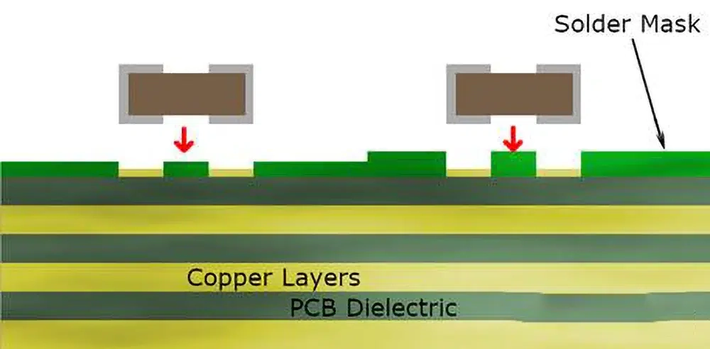
Solder masks add a layer of durability. They protect the board from physical damage. This means PCBs last longer. It also means fewer repairs and replacements. Overall, they improve the reliability of electronic devices.
Solder masks make PCBs look neat and clean. They come in different colors, such as green, blue, and red, which can help identify different boards. Beyond appearance, they also make inspection easier. The contrast between the mask and the traces makes it easier to spot issues.
In summary, solder masks are indispensable. They provide protection, prevent problems, enhance reliability, and improve appearance. With them, our electronic devices are more reliable.
There are different types of solder masks, each with its own advantages and ideal uses. Let's explore the main types in detail.
Liquid epoxy solder masks are the most commonly used type. They are made from polymers and applied using the Screen Printing (Silk Screening) method.
This process is similar to printing a pattern on a T-shirt. The epoxy is pushed through a screen onto the PCB, covering the copper traces and pads.
LPI solder masks offer higher precision than epoxy types. They consist of a mixture of polymers and solvents, applied to the PCB via screen printing or spraying.
After application, the board is exposed to ultraviolet (UV) light through a photomask, which defines the areas where the solder mask should remain. The exposed areas harden, and the rest is washed (developed) away.
Dry film solder masks are excellent for high-density and high-precision PCBs. These masks are vacuum-laminated onto the board.
After lamination, the PCB is exposed through a photomask, similar to the LPI process. The exposed areas harden, and the unexposed film is removed to reveal the pads.
Top and bottom masks are applied to both sides of the PCB to identify areas for component placement and soldering. These masks cover the entire board surface except for the soldering areas.
Choosing the right solder mask depends on various factors. Consider the complexity of your PCB design, budget, and required precision.
Each type of solder mask has its unique strengths and weaknesses, so matching the mask to your specific needs is essential to ensure optimal performance and durability of your PCB.
By understanding the different types of solder masks and their applications, you can make an informed decision that enhances the reliability and functionality of your electronic devices.
Applying a solder mask involves several steps. Each step is crucial to ensure the mask functions properly.
First, the PCB must be cleaned. Dirt and grease can cause problems. Cleaning removes these contaminants. This step ensures the solder mask adheres well. Standard methods include chemical cleaning and scrubbing.
Next, the solder mask ink is applied. There are two main techniques.
Both methods cover the copper traces and pads.
After coating, the board needs pre-curing. This step slightly hardens the ink. It prepares the board for the next step. Pre-curing can be done using heat or ultraviolet light. It ensures the mask stays in place during the imaging process.
Now, the board undergoes imaging. A photomask is placed on the board. Ultraviolet light is shone on it. The light hardens the exposed areas.
Alternatively, laser imaging can be used. This method is precise and does not require a photomask. Both methods define the final pattern of the solder mask.
Next is developing and rinsing. The board is washed to remove unhardened ink. This reveals the copper pads where components will be soldered. Developing is crucial. It ensures only the desired areas are exposed, while the rest of the board remains protected by the solder mask.
The final step is final curing. The board goes through a final hardening process, which fully cures the solder mask, making it durable and long-lasting. After curing, the board is cleaned again. This removes any residue and ensures the board is ready for the next step in manufacturing.
In summary, every step in the solder mask application process is vital. From cleaning to final curing, each stage ensures the solder mask performs its function correctly, protecting the PCB and enhancing its performance.
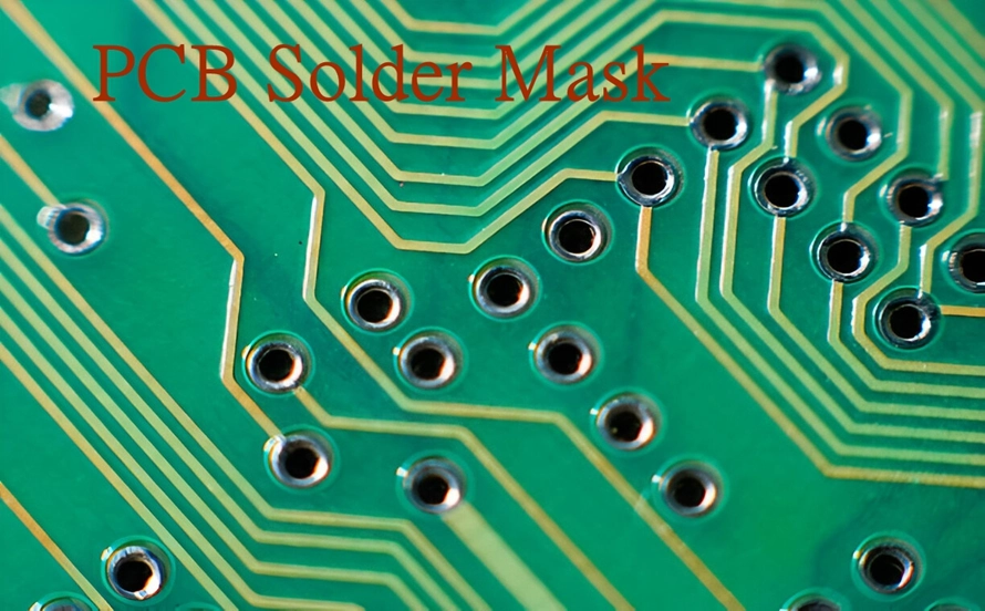
When designing a PCB, the solder mask is crucial. Let's look at the key factors to consider.
Clearance is the space between the solder mask and the copper pad. It's important for preventing short circuits. If the mask is too close, solder can bridge the gap.
Standards help guide this spacing. Typically, a clearance of 4 mils is used for green solder masks and 5 mils for other colors. This spacing ensures safety and functionality.
Thickness is important. The standard thickness is about 0.8 mils. If it's too thin, the mask may not protect the copper sufficiently. If it's too thick, it might cause problems during assembly.
Proper thickness ensures the mask is effective without affecting the PCB's performance. It protects the board while facilitating soldering.
Green is the most common color. It's popular because it provides good contrast and visibility. Other colors include red, blue, yellow, black, and white. Each color can help differentiate between different boards or layers.
Finishes can be glossy or matte.
The choice depends on the application and visual needs. Glossy is often used for aesthetic purposes, while matte is preferred for inspection and handling.
When designing with solder masks, consider clearance, thickness, color, and finish. These factors ensure the mask performs well and the PCB functions properly. Making the right choices leads to reliable and durable PCBs.
Solder masks are crucial for PCBs. They prevent oxidation and short circuits. They also add durability and improve the board's appearance. With them, PCBs are more successful.
Choosing the right solder mask is vital. Consider your PCB design and needs.
Want to learn more? Need assistance with your PCB design? Contact us for professional help. We are committed to ensuring your PCBs are reliable and of high quality.
Thank you for reading! Please feel free to contact us with any questions or comments.
