November 28, 2025
Wherever electronic products exist, PCBs (printed circuit boards) are indispensable. Industry veterans often mention “positive film” and “negative film.” If you're as confused by these terms as I was when I first entered the field as a rookie 20 years ago, let's discuss the differences between these two manufacturing processes today.
Simply put, the main difference between positive and negative processes lies in PCB plating and image transfer methods. Once image transfer (creating the circuit pattern) is completed, the subsequent processes (such as solder mask, legend printing, etc.) are largely similar.
The fundamental difference between positive and negative processes lies in whether it's "what you see is what you get" or "what you see is the opposite (reverse)", and whether it uses "subtractive" or "additive" methods.
Below, I'll use a typical 4-layer board as an example to provide a detailed analysis covering definitions, process flows, advantages/disadvantages, and application scenarios.
After applying photosensitive dry film, exposure, and developing, the copper surfaces revealed after developing are the ones we don't need. These exposed copper areas are subsequently etched away by acidic etching solution. The circuit patterns we need are protected by the dry film. After etching is completed and the protective dry film is stripped away, the circuit is formed.
Industry Terminology:
Front-end Design → Panel Cutting (Material Preparation) → Inner Layer Circuit Fabrication (Negative) → Lamination → Drilling → Electroless Copper (PTH) → Panel Plating (Primary Copper, plated to full thickness) → Pre-treatment → Lamination → Exposure → Developing → Acidic Etching → Stripping → Back-end Processes (AOI Optical Inspection)
Memory Point:
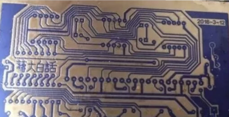
After lamination, exposure, and developing, the copper surfaces revealed after developing are exactly the circuit areas we need. The areas covered by dry film are the unwanted copper.
The exposed copper after developing is typically thin, so we perform Pattern Plating (secondary copper) to thicken the circuits, followed by plating a layer of tin or tin-lead as an anti-etching protective layer.
After plating copper and tin, first strip the dry film to reveal the unwanted copper surfaces, then use alkaline etching solution to etch away these unprotected copper areas. Finally, strip the tin layer protecting the circuits to complete circuit fabrication.
Industry Terminology:
Front-end Design → Panel Cutting → Inner Layer Fabrication → Lamination → Drilling → Electroless Copper (PTH) → Panel Plating (Primary Copper, thin copper base) → Pre-treatment → Lamination → Exposure → Developing → Pattern Plating (Secondary Copper Thickening) → Tin Plating (Protective Layer) → Stripping → Alkaline Etching → Tin Stripping → Back-end Processes (AOI)
Memory Point:
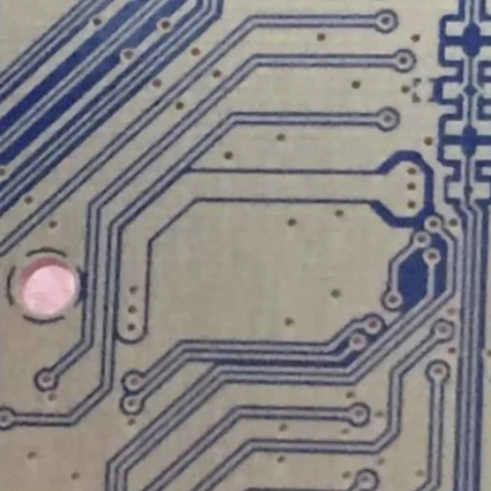
You can think of PCB manufacturing process as similar to traditional camera "photo developing":
This difference mainly occurs during the "image transfer" and "etching" stages.
Positive (for outer layers): Like "addition". First determine positions, then "put armor on circuits" (tin plating), then eliminate enemies without armor (excess copper) with alkaline etching. High precision, suitable for outer layer routing and through-holes.
Negative (for inner layers): Like "subtraction". First cover areas to be preserved with dry film, then eliminate all unwanted copper at once with acidic etching. Low cost, fast speed, suitable for inner layer fabrication.
In modern PCB manufacturing (especially multi-layer boards), mixed usage is common:
Hope this detailed explanation helps you thoroughly understand the difference between positive and negative processes!
The above discussion is for reference only. Each PCB manufacturer has different chemical characteristics, process capabilities, equipment parameters, and product structures, so don't apply these concepts rigidly. All effective process improvements must be based on data and verified through DOE experiments - this is the professional approach for engineers.
