July 21, 2026
As data rates push toward 56G/112G PAM4 and operating bands extend from Sub-6 GHz into millimeter wave, the laminate is no longer a mechanical carrier — it is an electrical component that directly shapes system performance. Many R&D teams share the same experience: the simulation looks clean, but the fabricated board measures 1–2 dB worse on insertion loss. The root cause is often not the layout, but a parameter overlooked during material selection. This article organizes the six engineering criteria that actually decide success in high-speed and high-frequency material selection, along with the relevant IPC framework.
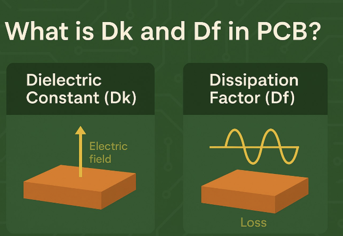
The dielectric constant (Dk) determines how fast electromagnetic energy propagates through the substrate. Lower‑Dk materials mean faster signals and less propagation delay — critical for timing alignment across multi‑lane serial interfaces and wide parallel buses. Higher Dk slows propagation and amplifies skew, especially when signals cross multiple layers or mixed materials.
More important than the absolute value is stability. Today's digital signals carry frequency content well into the tens of gigahertz; any Dk drift across frequency, temperature, or material orientation introduces timing dispersion and eye closure. Rough practical boundaries: enhanced FR‑4 shows growing Dk variation at higher frequencies, limiting practical use to roughly 3–10 GHz; hydrocarbon‑ceramic composites hold stable through 10–30 GHz; PTFE and Megtron 6/7‑class materials deliver the Dk stability required for 56G/112G PAM4 and mmWave.
One frequently missed detail is dielectric anisotropy: most modern laminates have different Dk in the x‑y plane versus the z‑axis. Accurate modelling of microstrip, stripline, and resonant structures requires directional Dk data — not a single catalog number.
If Dk sets velocity, dissipation factor (Df) sets how far a signal can travel. As frequency rises, dielectric loss dominates insertion loss and compresses usable channel length in backplanes and dense interconnects — with especially sharp impact on PAM4 eye height. In RF designs, elevated Df drags down Q‑factor and radiation efficiency.
There's a trap when comparing Df: suppliers may quote values at 1 GHz or 10 GHz, measured by different methods. Only data derived under identical IPC‑TM‑650 methods are comparable; building a loss budget from mismatched test data is a common root cause of simulation‑to‑hardware mismatch.
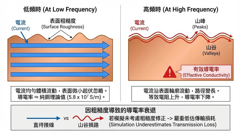
With the dielectric optimised, the practical ceiling at high frequency often sits in the conductor. Skin effect forces current into a thin surface layer of copper; foil roughness lengthens the effective path and raises resistance, directly increasing attenuation — affecting achievable data rate, maximum channel length, RF insertion‑loss slope, and jitter.
IPC‑4562 defines the copper foil classes: standard electrodeposited (ED), very‑low‑profile (VLP), hyper‑VLP (HVLP), and rolled‑annealed (RA). VLP/HVLP foils cut loss significantly versus standard ED; RA copper is the smoothest and is common in ultra‑low‑loss and flex applications.
Surface finish carries real weight too: ENIG introduces extra high‑frequency loss because of nickel's poor RF conductivity, while OSP and immersion silver preserve a smoother copper interface and generally perform better at speed. Rule of thumb: above roughly 2.4 GHz, or when interconnects reach tens of centimetres, surface finish becomes a meaningful contributor to total loss.
High‑frequency systems routinely operate under elevated temperature, thermal cycling, and vibration, so electrical performance needs thermal/mechanical backing. Three core parameters: glass transition temperature (Tg) for resin stability, decomposition temperature (Td) for lead‑free soldering robustness, and coefficient of thermal expansion (CTE) for via fatigue and barrel‑cracking risk. In hybrid stackups — especially FR‑4 co‑laminated with PTFE or ceramic materials — CTE mismatch causes mechanical stress, timing drift, and even delamination. For acceptance, IPC‑6012 (rigid) and IPC‑6018 (RF/microwave) apply; the latter imposes tighter controls on dielectric uniformity and copper adhesion and is the relevant standard for speed‑critical builds.
| Material family | Characteristics | Typical range | | :--- | :--- | :--- | | Enhanced FR‑4 | Better Dk control and Df than standard FR‑4, higher Tg | ~2.5–10+ Gbps; RF below ~3–6 GHz | | Hydrocarbon‑ceramic composites (e.g., Rogers RO4350B) | Low loss with better manufacturability; suits hybrid stackups | 10–40 GHz RF; 10–56+ Gbps | | PTFE laminates | Ultra‑low loss, stable Dk; higher cost and process complexity (IPC‑4103) | 30–110+ GHz, antennas, radar | | Panasonic Megtron series | Low Df, strong thermals, compatible with conventional processes | 25G/56G/112G — switches, backplanes, HPC |
Regulatory risks: PFAS‑containing PTFE laminates face a proposed broad restriction by the European Chemicals Agency (ECHA) under REACH, which could impact supply continuity if enacted. Certain Megtron formulations may contain DBDPE (decabromodiphenyl ethane), classified as a Substance of Very High Concern (SVHC) under REACH. Products targeting the European market should verify material declarations early.
Advanced materials often require non‑standard processing. PTFE is especially demanding: plasma or sodium‑etch surface treatment, specialised drilling parameters, modified desmear, and sometimes fusion bonding. A factory without experience on a given material system will give back voids, roughened copper, poor adhesion, and dimensional instability — eating the performance the model promised. That is why aligning process capability with the manufacturer before the stackup is frozen (IPC‑2221/2222 provide the DFM framework) is the precondition for realising modelled performance in production.
Consistency across builds and suppliers ultimately relies on documentation, not habit. Stackup documentation should explicitly define: the IPC‑4101/4103 slash sheet, dielectric thickness and resin content, target Dk/Df, copper foil class per IPC‑4562, impedance requirements with IPC‑TM‑650 methods, the applicable acceptance standard (IPC‑6012 or 6018), and any special processing needs.
In our material‑selection reviews with customers, the three most common blind spots are: reading catalog Dk without checking frequency dependence and anisotropy, comparing Df values measured by different test methods, and choosing a material system the factory has never run in volume.
eCloud provides integrated services from prototyping to complex HDI builds, with deep experience across high‑speed networking, silicon photonics, edge AI, and RF applications. Defining a stackup for your next high‑speed or RF project? Talk to our engineering team at the layout stage for material‑selection and DFM pre‑review input — and converge your loss budget and sourcing risk in one pass.
