PCB board profiling is the process of machining a PCB manufacturer's Working Panel into the final size and shape required by the customer. In this process, selecting the appropriate profiling method is crucial, as different processing techniques each have their own advantages and disadvantages in terms of accuracy, efficiency, cost, and applicable scenarios. Choosing the wrong method can lead to dimensional deviations, burred edges, or even batch scrapping, causing unnecessary losses for the enterprise.
Explanation of Common Terms in the PCB Manufacturing Industry
To understand profiling processes, we first need to clarify several key dimensional definitions in PCB manufacturing:
- Sheet (Panel Sheet):
- Refers to the shipment form of the CCL (Copper Clad Laminate) substrate.
- Common Sheet sizes in PCB factories include 43" x 49", 41" x 49", 37" x 49", etc.
- The board house will cut the Sheet into different Panels according to requirements.
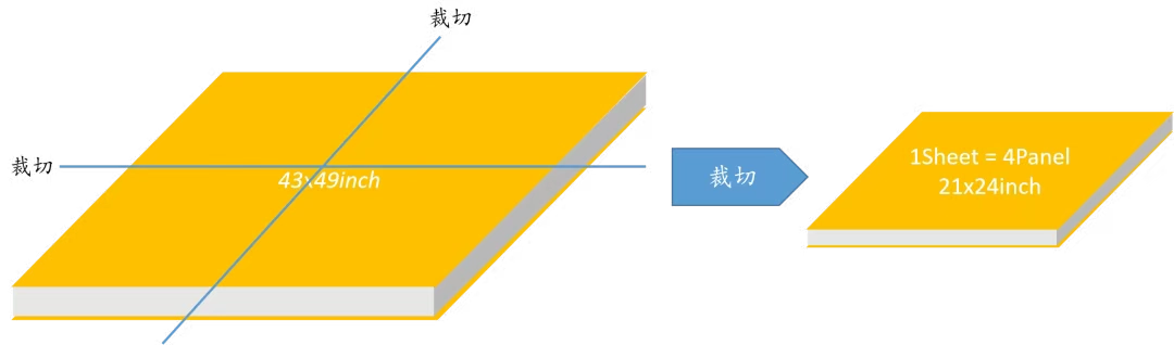
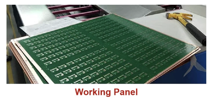
- Working Panel (WPNL):
- The Panel used for PCB production input, abbreviated as WPNL.
- Common WPNL sizes are, for example, 21" x 24", 20" x 24", 18" x 24", etc.
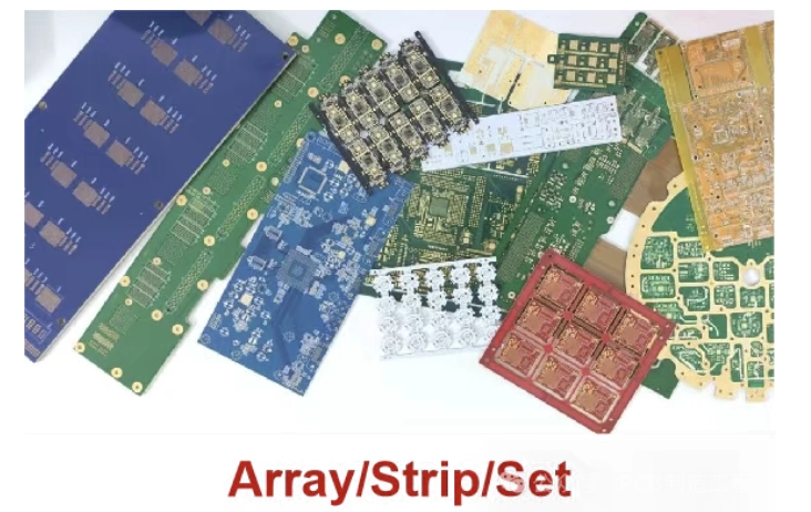
- Array (or Strip, Set, Shipping Panel / SPNL):
- Usually designed by the customer, often the smallest shipping form of the PCB, composed of multiple units.
- Unit (PCS, Card, or Unit):
- The smallest unit of a PCB board.
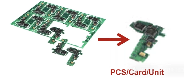
Note: For larger-sized PCB boards, there might be no Array, only a Unit. This means a single unit is the shipping panel, especially common for PCBs with large unit sizes.
Definition and Purpose of PCB Board Profiling
In simple terms, PCB board profiling involves creating a program based on the customer-defined outline. Then, machines are used to process the PCB factory's Working Panel into the delivery unit required by the customer, such as an Array (or Strip) or a Unit (PCS, Card, or Unit).
The purpose of this process is to ensure that the final circuit boards delivered to the customer match the design drawings exactly in terms of their outline dimensions.
Common PCB Profiling Methods
The choice of profiling method directly affects the edge quality, precision, and production efficiency of the PCB. Common profiling methods include:
- Routing: Includes mechanical routing and laser cutting; this is the most common method for cutting irregularly shaped boards.
- Routing with Beveling (Chamfering): After routing is complete, the edges are beveled for specific assembly requirements.
- V-Cut (V-Scoring): Primarily used for pre-scoring straight or rectangular boards to facilitate subsequent breaking by the customer.
- Routing with V-Cut: Combines both methods, using routing for the overall outline and V-Cut for internal units or specific straight edges.
- Routing with Controlled-Depth Routing: Uses a depth-controlled tool for routing to ensure specific depth requirements are met.
- Punching: Uses a die to stamp and form the board in one action, suitable for high-volume production, products with less stringent precision requirements, or specific shapes.
A profiling workflow diagram involves the collaborative work of multiple steps to ensure the WPNL is correctly converted into the customer's required unit size.
1. Mechanical Routing (Milling)
- Definition: Mechanical routing, also called milling, involves creating a program (also called a routing program) based on the customer's requirements for PCB board size. After inputting this program into the routing machine, a CNC (Computer Numerical Control) system controls the router to perform precise routing using an end mill (also called a router bit).
- Characteristics: This is the oldest, most widely used, and lower-cost profiling method in the industry.
2. Laser Cutting
- Definition: Laser Cutting is a technology that uses a laser to cut materials into specific shapes specified by the customer.
- Working Principle: A high-power laser beam is guided through an optical system and directed onto the workpiece. This causes the irradiated material to rapidly melt, vaporize, or ablate. Simultaneously, a coaxial high-speed gas jet blows away or extracts the molten material, achieving the cut.
- Control System: A motion control system follows CNC programming language (G-code or M-code) to guide the laser beam along the intended cutting path.
- Advantages of PCB Laser Cutting (vs. traditional mechanical routing):
- High Precision and Small Kerf: Small cutting gap and high precision.
- Small Heat-Affected Zone (HAZ): Minimal thermal impact on the surrounding material.
- Excellent Edge Quality: Laser-cut PCBs are dust-free, stress-free, and burr-free, with smooth and neat cut edges.
- Wide Applicability: Particularly suitable for processing complex shapes.
3. V-Cut (V-Scoring) Process
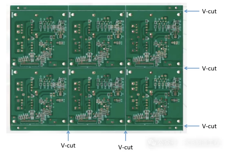
- Definition: V-Cut, also called V-scoring, uses specialized V-Cut equipment to create a V-shaped groove between multiple PCB units. This allows the customer to conveniently and efficiently break the PCB from an Array into individual Units after component assembly is complete.
- Applicable Scenarios: Suitable for PCB boards with relatively regular shapes. Both V-Cut alone and V-Cut combined with routing are common PCB board profiling methods.
- Key Parameters: Depth (D), Angle (θ) (common values: 30°, 45°, 60°), Remaining Thickness (Web), and front-to-back positional offset.
4. Controlled-Depth Routing
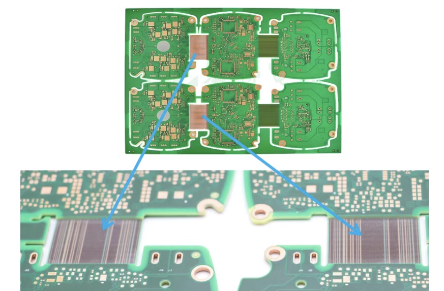
- Definition: Controlled-depth routing is commonly seen in rigid-flex PCBs. It utilizes the depth control function of a profiling machine to precisely route away the rigid board portion covering the flexible circuit area, exposing the flex.
- Other Applications: This design also exists in other products, such as stepped blind slots, mechanically controlled-depth blind holes, etc.
- Key Considerations:
- Depth Control: Affected by many factors, such as equipment precision, router bit material and angle, dielectric thickness tolerance, board warpage, etc.
- Precision Control: Positioning for controlled-depth routing can be based on hole location or pad location, depending on accuracy requirements.
5. Punching Process
- Definition: Punching, also known as die-cutting or stamping, is a fast profiling method, but the die costs are relatively high.
- Characteristics: The advantage is rapid profiling, but the upfront mold development cost is high. Therefore, punching is typically used only when the PCB production volume is very large.
Profiling Process Comparison Summary
| Profiling Process | Suitable for Prototypes | Suitable for Mass Production | Key Characteristics |
| :--- | :---: | :---: | :--- |
| Mechanical Routing | ✔ | ✔ | Traditional method, most widely used, low cost. |
| V-Cut | ✔ | ✔ | Common profiling method, suitable for PCBs with relatively regular shapes. |
| V-Cut + Mechanical Routing | ✔ | ✔ | Higher efficiency compared to routing alone. |
| Beveling + Mechanical Routing | ✔ | ✔ | Often used for PCBs with gold fingers or other plug-in features. |
| Laser Cutting | ✔ | ✔ | High precision, suitable for PCBs with complex shapes, higher cost. |
| Controlled-Depth Routing/Laser | ✔ | ✔ | Common for rigid-flex PCBs and boards with special requirements. |
| Punching | | ✔ | Suitable for large-scale mass production, fast profiling, high mold cost. |
Conclusion
In summary, the PCB board profiling process is the final critical step determining the ultimate quality, performance, and manufacturing cost of electronic products.
From the traditional and widely used mechanical routing, to the convenient and efficient V-Cut, to laser cutting for complex shapes and punching for mass production, each profiling method has its unique technical advantages and application scenarios.
Manufacturers must carefully select the most appropriate profiling solution based on the product's design requirements, precision needs, and expected production volume. Only precise profiling processes can ensure that the delivered PCB products perfectly meet the customer's assembly and functional requirements.
