December 8, 2025
Key Manufacturing Technologies for Enhancing High-Speed Signal Integrity
In the fields of high-speed digital circuits and RF/microwave applications, signal integrity in printed circuit boards (PCBs) is critical. Back Drilling (also called Controlled Depth Drilling) is a specialized PCB manufacturing process that significantly improves signal integrity by removing excess via stubs. It is an indispensable key technology in modern electronics manufacturing.
This article will provide a detailed analysis of the back drilling process, covering its definition, working principles, application scenarios, specific procedures, and key control points.
Back Drilling, also known as Controlled Depth Drilling or Back Drilled Holes, is a PCB manufacturing process. Its purpose is to perform a second drilling operation to remove the excess copper barrel portion in a multilayer board's through-hole that is not connected or used for signal transmission. This excess copper barrel is called the "Stub".
When a signal only needs to travel from the first layer (L1) to the ninth layer (L9), a conventional through-hole results in the hole wall being plated with copper all the way from L1 to the bottommost layer. The portion from below L9 to the bottom layer becomes the excess stub.
In high-frequency signal transmission, this stub acts like an antenna, causing radiation effects that lead to signal reflection, scattering, and delay, degrading signal integrity. The Back Drilling Process involves a second, precisely controlled drilling operation from the back (or front) side of the PCB to accurately remove this excess stub portion.
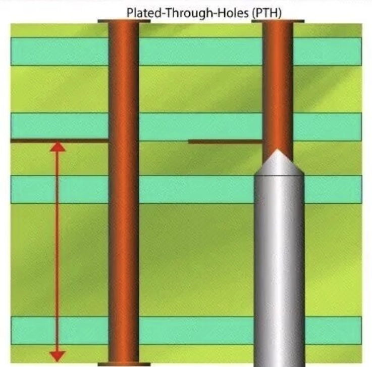
The core principle of back drilling is to use a drill bit with a diameter slightly larger than the original via to perform a controlled-depth drilling operation from one side of the board, precisely removing the excess copper barrel while preserving the electrical connection of the required portion.
The back drilling depth can be calculated using a formula: Back Drill Depth = Total PCB Thickness - (Distance from Termination Layer to Board Bottom) ± Process Compensation Value.
For example: A PCB has a total thickness of 1.6 mm. To remove the stub below L5 in a hole connecting from the surface layer (L1) to L5, the back drill depth should be: "Thickness from L1 to L5 + 0.05 mm compensation" (to avoid damaging the L5 layer).
Back drilling technology is primarily used in high-speed circuit applications with demanding signal integrity requirements:
Cost Consideration: Back drilling increases PCB manufacturing cost by approximately 20% to 30%. However, for high-speed (typically >5 Gbps) signal applications, it is one of the most cost-effective solutions.
The back drilling process consists of the following main steps:
This process flow ensures back drilling precision and avoids quality issues arising from multiple processing steps.
Successful implementation of the back drilling process requires strict control over the following key points:
Depth control is the core of the process. The allowable deviation is typically controlled within ±0.05 mm, with high-frequency boards even requiring high precision of ±0.025 mm.
Control measures include:
The alignment accuracy between the back drill hole and the original hole position is critical. Excessive deviation can damage inner layer circuits.
Improvement methods include:
Quality verification after back drilling is equally important. Main inspection methods include:
The essential difference between back drilling and traditional drilling lies in its characteristics of being "secondary, depth-controlled, and subtractive." Its implementation principle is far from simply "drilling shallower"; it is a sophisticated system integrating high-precision mechanics, sensing technology, software compensation, and materials science.
To understand their difference, one must first recognize their completely different purposes.
| Process | Analogy | Purpose | | :--- | :--- | :--- | | Traditional Drilling (Primary Drilling) | Like pouring a water pipe from the rooftop down to the basement when building a house | To allow the conductive path to run from the top layer through to the bottom layer | | Back Drilling (Controlled Depth Drilling) | Like precisely drilling upwards from the basement after the house is built to cut off that unused section of pipe | To remove the useless stub while absolutely avoiding damage to the effective conductive via wall that is still needed |
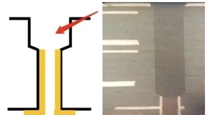
The realization of back drilling centers on "depth control," which is a systematic engineering feat.
Special Note: Some factories produce controlled-depth blind holes using mechanical drill bits, which are also called "back drill holes." These blind holes generally have a relatively large diameter (0.3 mm to 3.0 mm), distinctly different from the diameter of laser-drilled blind holes (typically 0.075 mm to 0.3 mm).
The back drilling process significantly enhances signal integrity in high-speed PCBs by removing excess stubs from vias, thereby reducing reflection and interference. Its implementation relies on high-precision electromechanical systems, precise sensing and positioning, complex software algorithms, and rigorous process management.
Mastering the principles, procedures, and key control points of back drilling technology is of great significance for designing and manufacturing high-performance electronic equipment.
The above discussion is for reference only, intended to initiate thought. Each factory's processes, equipment, and product structures have their own differences. All effective improvement measures should be based on experimental data.
Source: Compiled from internet resources for the purpose of knowledge exchange and learning.
