We can compare a standard PCB to a "single-story bungalow" where traces can only be laid on the same plane. In contrast, an HDI board is like a "loft apartment": not only can components be mounted on the surface, but tiny vias can connect the "inter-layer wiring," significantly improving space utilization. This is the core value of HDI: "small space, high utilization."
This article will provide an in-depth analysis of the technical foundations, core advantages of HDI PCBs, and explore the challenges and key considerations in their design.
1. Technical Foundation of High-Density Interconnect PCBs
High-Density Interconnect (HDI) PCBs are printed circuit boards that possess higher circuit density and miniaturization capabilities compared to traditional PCBs. Their design goal is to accommodate more components and connections in a smaller space.
Core Characteristics of HDI
- High Wiring Density: HDI PCBs have more connection points in a smaller area. Their trace width and spacing can achieve 0.05 to 0.1 mm (thinner than half a human hair). In the same area, they can accommodate 2 to 3 times more traces than a standard PCB.
- Microvias: These are tiny holes connecting different layers of the PCB, typically with diameters less than 0.15 mm, enabling more precise interconnections.
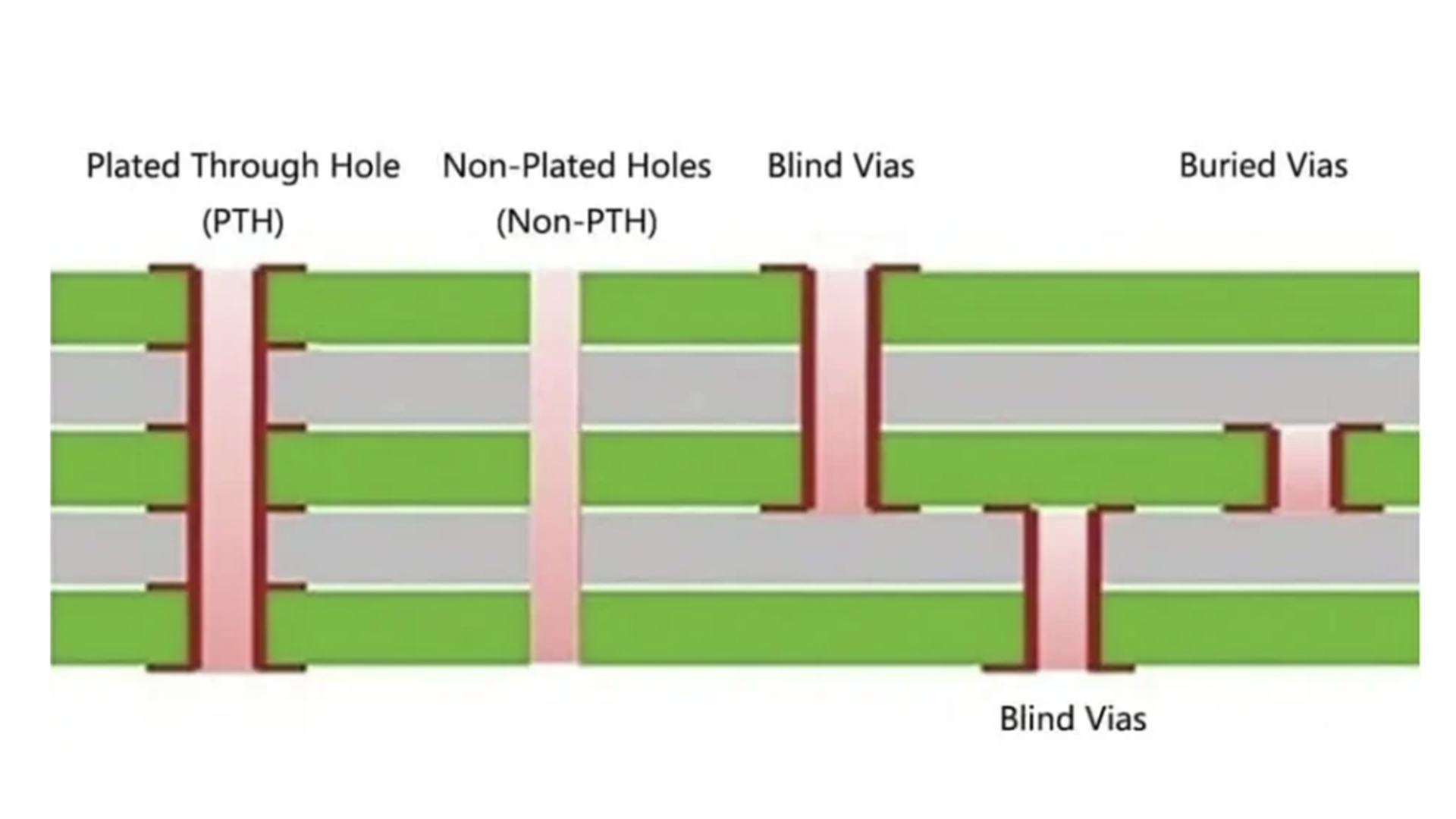
- Blind Vias and Buried Vias: These technologies save space on the board.
- Blind Vias: Connect an outer layer to an inner layer but do not penetrate the entire board.
- Buried Vias: Connect inner layers and are completely encapsulated within the board.

2. Core Advantages and Application Fields
1. Compactness, Lightweight, and High Integration
HDI PCB thickness typically ranges from 0.4 mm to 1.0 mm, much thinner than standard PCBs (commonly 1.6 mm). Through the use of microvias, blind vias, and buried vias, a single board can integrate more functional modules, achieving higher functional density.
2. Superior Performance and Enhanced Reliability
- Better Signal Integrity (SI): Signal transmission paths are shorter, reducing signal degradation and parasitic capacitance/inductance effects. This is crucial for high-speed data transmission applications such as 5G communications, data centers, and automotive electronics.
- Enhanced Electrical Performance: Improved impedance control precision makes them more suitable for demanding applications like satellite communications and high-speed computing.
3. Long-Term Cost-Effectiveness and Environmental Considerations
- Reduced Material and Layer Count: By efficiently utilizing space, HDI technology allows PCBs to achieve functionality with fewer layers, thereby reducing material costs and providing long-term production cost savings through manufacturing efficiency.
- Environmental and Health Benefits: Many HDI PCBs use lead-free solder, enhancing manufacturing safety and reducing environmental impact.
3. Differentiating Features: HDI PCB vs. Traditional PCB
| Feature | HDI PCB (High-Density Interconnect) | Traditional PCB (Standard) |
| :--- | :--- | :--- |
| Circuit Density | Extremely high, with very fine trace widths and spacing (less than 0.1 mm). | Lower, limited by the number and density of wiring layers. |
| Hole Size | Microvia diameter typically less than 0.2 mm, smaller than a sesame seed. | Through-hole diameter typically ≥ 0.3 mm. |
| Performance | Excellent signal integrity, suitable for high-frequency, high-speed applications. | Signal attenuation and parasitic effects are relatively more pronounced. |
| Manufacturing Process | Requires advanced processes like laser drilling and sequential lamination. | Primarily uses mechanical drilling and single-stage lamination processes. |
4. HDI PCB Structure and Key Manufacturing Processes
The complex structure of HDI PCBs is achieved through advanced design techniques and specialized manufacturing processes.
1. Core HDI Interconnection Technologies
- Microvias: Diameter less than 0.15 mm, the foundation for achieving high density in HDI.
- Blind Vias: Connect outer layers to inner layers without penetrating the entire board.
- Buried Vias: Completely encapsulated within the board, connecting inner layers.
2. Laser Drilling and Sequential Lamination Process
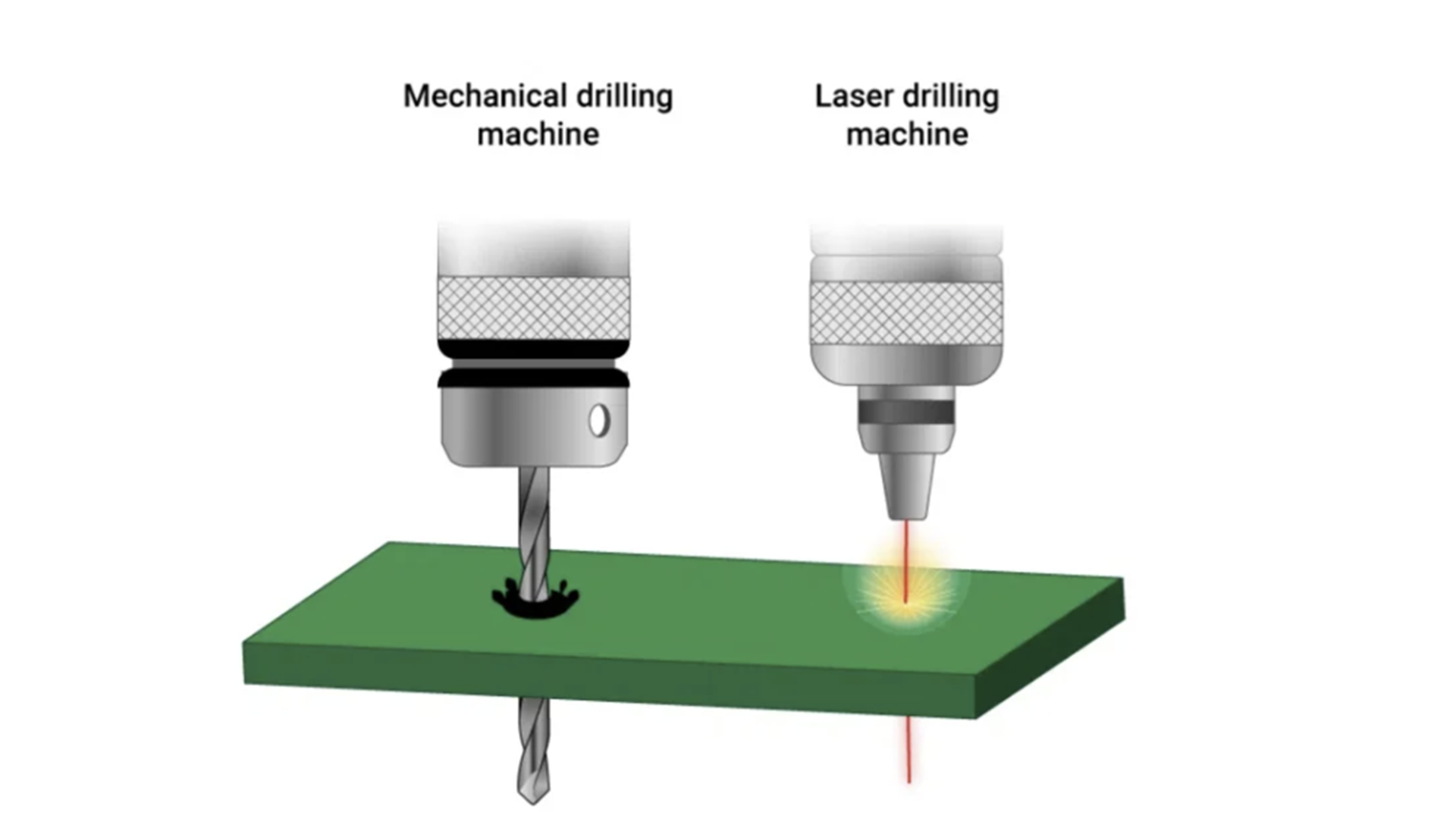
- Laser Drilling: Key to creating microvias. Standard PCBs can only mechanically drill holes larger than 0.3 mm, while HDI uses laser drilling to precisely create holes as small as 0.1 mm. Laser-drilled holes have exceptionally smooth edges, avoiding burrs common in mechanical drilling and effectively preventing short circuits.
- Sequential Lamination: A defining feature of HDI. HDI boards are not fabricated all at once; they are built up layer-by-layer like "stacking a cake." First, the bottom layer circuitry is made, then a thin substrate is added, laser microvias connect to the bottom layer, followed by the next layer's circuitry, and so on. This sequential build-up allows for greater precision in inner layer traces and effectively controls layer-to-layer alignment deviation in multi-layer boards.
3. Coreless Construction and Design Standards
- Coreless Construction: Involves using paired layers without a central core, helping achieve thinner, more flexible designs.
- Design Standards: Design and manufacturing must adhere to industry standards such as IPC-2315, IPC-2226 to ensure quality and performance.
5. HDI PCB Design and Manufacturing Challenges
- Manufacturing Process Limitations: Processes like laser drilling and sequential lamination require specialized equipment, increasing manufacturing costs. The number of manufacturers with HDI mass production capabilities is limited.
- Signal Integrity Management: High-density routing is prone to crosstalk. Simulation tools are needed to optimize differential pair routing and termination strategies, and transmission line parameters must be strictly matched to control high-frequency losses.
- Thermal Management Challenges: Increased power density leads to significant heat dissipation pressure. Solutions include thermal vias, metal-core substrates, and heat sinks for enhanced thermal conduction, along with early-stage thermal simulation in the design phase.
- Complexity of Design Rules: Microvia parameters (e.g., aspect ratio, annular ring) must meet strict requirements such as the IPC 6012 Class 3 standard.
- Design for Manufacturability (DFM): Requires collaboration with the manufacturer to define minimum trace width/spacing, stack-up structure, and to balance the high cost of advanced HDI with budget constraints.
6. HDI PCB Grade Classification and Identification
1. Relationship Between Blind/Buried Vias and HDI
HDI boards are high-density interconnect boards. Boards with blind vias that are plated and then undergo secondary lamination are HDI boards. Simple buried vias do not necessarily constitute an HDI board.
2. Grade (Level) Classification
HDI technology levels are distinguished by "grades" (1st, 2nd, 3rd order, etc.):
- 1st Order HDI: The simplest, with relatively easy process flow and control.
- 2nd Order HDI: Increased complexity. Several primary design approaches exist, including staggered, stacked, or directly drilling from the outer layer to the N-2 layer.
- 3rd Order and Above: Technical difficulty and cost increase significantly (e.g., iPhone motherboards often use 5th order HDI).

3. How to Quickly Identify an HDI Board
- Look at Hole Size: Using a magnifying glass, if the holes appear as small as sesame seeds (less than 0.2 mm), it is essentially an HDI board.
This article provided an in-depth exploration of the fundamentals and applications of HDI PCBs. Tomorrow, we will continue with subsequent related HDI technologies. Stay tuned.
