PCB Specification Evolution and Cross-Domain Cost Calculation in Product Development
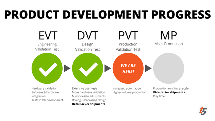 This article will break down the PCB specification requirements and cost calculation logic for each stage in conjunction with the product development cycle, and deeply analyze why boards in different industries are so expensive. This will help you keep a clear financial and manufacturing roadmap in mind when you route that very first trace.
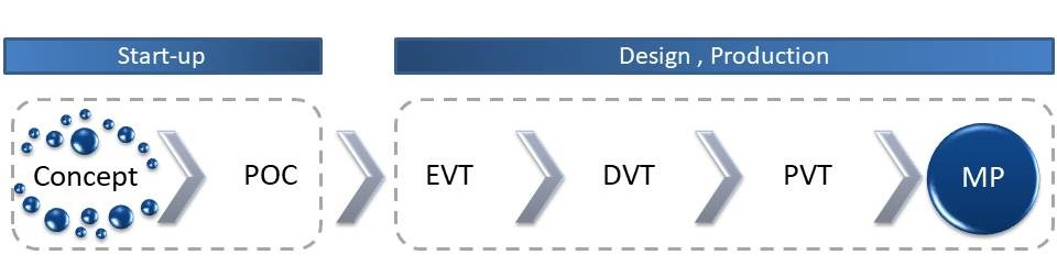
I. PCB Specification Evolution and Cost Logic in the Four Stages of Development
Hardware development is a game of “buying information with money and reducing risk through stages.” The PCB in each stage has its milestone tasks. Never use mass‑production standards for prototyping, and never apply the casualness of prototyping to mass production.
1. POC (Proof of Concept) Stage: Speed over Unit Price
- Stage Goal: Core technology feasibility verification.
- PCB Specification Requirements: Almost no strict stack‑up restrictions. To get the board as fast as possible, standard stock materials from the board manufacturer, the loosest trace widths and spaces, and even flying wire (jumper) modifications are totally acceptable.
- Cost Calculation Logic: The core cost here is “time.” Although the engineering fee for prototyping is extremely high when spread over a single board, the total amount is very low. At this stage, absolutely do not spend time on extreme DFM optimisation; getting the board with the fastest lead time to write firmware is king.
2. EVT (Engineering Verification Test) Stage: Specification Convergence, Real Stack‑up Online
- Stage Goal: Complete functional verification and electrical defect elimination.
- PCB Specification Requirements: You must begin using the product’s final intended stack‑up and materials. Impedance control for high‑frequency signals must be precisely implemented at this stage, and component footprints must be consistent with future mass production.
- Cost Calculation Logic: EVT will go through multiple revisions. The hidden costs at this stage lie in the “frequent prototyping engineering fees” and “debugging time.” An initial DFM review must be initiated now to ensure that the specific high‑frequency material or special thickness you choose is not a scarce commodity in the market; otherwise, it will bring huge supply chain risks later.
3. DVT (Design Verification Test) Stage: Certification‑Driven, Material and Panelisation Locked
- Stage Goal: Reliability verification and global safety certifications.
- PCB Specification Requirements: By DVT, the PCB’s Bill of Materials (BOM) and stack‑up must be completely frozen. The boards will be sent to labs for extreme high/low temperature, ESD, drop, and other destructive tests. Any minor tweaks to the material model or routing could cause hundreds of thousands of dollars in certification fees to go down the drain.
- Cost Calculation Logic: The cost focus shifts from prototyping fees to “fixtures” and “panel utilisation.” Layout engineers must confirm the final array panelisation method, breakaway tab (tooling edge) design, and V‑cut routing direction with the board manufacturer at this time. If panel utilisation is below 80%, material costs will be wasted every single second in future mass production.
4. PVT (Production Verification Test) Stage: Focus on Yield, Eliminate Hidden Dangers
- Stage Goal: Production line assembly process verification and yield ramp‑up.
- PCB Specification Requirements: No design changes are allowed. Completely focused on solving process issues during component mounting, such as poor soldering (non‑wetting), board warpage, and deformation through the reflow oven.
- Cost Calculation Logic: Here we calculate “scale cost.” If the solder mask opening isn’t designed well, causing solder bridging and rework, or if too few Test Points are left, resulting in inefficient ICT (In‑Circuit Testing), these seemingly trivial matters in EVT will be amplified into million‑dollar production line waste in PVT.
II. Cross‑Domain PCB Complexities: Why Are Automotive and Aerospace So Expensive?
Having understood the evolution of the timeline, let’s look at the differences on the “spatial axis.” Even for an 8‑layer board, the design specifications and manufacturing costs for consumer electronics, automotive, medical, and aerospace PCBs belong to completely different dimensions.
1. Consumer Electronics: Extreme Space and Cost Squeezing
- Design Pain Points: Light, thin, short, small; short lifecycles; extremely cost‑sensitive.
- Specification Characteristics: Massive use of HDI blind/buried via technology to compress area; board thickness often challenges 0.8 mm or even thinner.
- Cost Focus: Cost depends on panel utilisation and the yield of blind/buried vias. Consumer product margins are razor‑thin; how many small boards can be cut from a large panel directly determines the product’s life or death. The supply chain will usually seek quotes from multiple board manufacturers; as long as basic electrical specs are met, whoever is cheapest gets the order.
2. Automotive: Harsh Extreme Environments and Zero‑Defect Commitment
- Design Pain Points: Continuous high temperatures and vibrations, lifecycles spanning over a decade, concerning human safety.
- Specification Characteristics: Mandatory requirement for High‑Tg materials to cope with engine compartment heat; heavy copper designs are widely used for high‑current paths; hole copper thickness requirements are far higher than general IPC standards.
- Cost Focus: The reason the cost doubles lies in extreme quality control and traceability. Automotive board manufacturers must hold IATF 16949 certification. Frequent cross‑section sampling, Automated Optical Inspection (AOI), and 100% electrical testing during production – these QA processes consume massive amounts of money. Furthermore, once suppliers and materials are locked for automotive parts, it is almost impossible to change them arbitrarily.
3. Medical Equipment: Precision Tolerances and Strict Regulations
- Design Pain Points: Signals are extremely weak and cannot be interfered with; life‑sustaining equipment has zero fault tolerance.
- Specification Characteristics: Extremely strict tolerance requirements for impedance control (often < 5%); special surface finishes may be needed to ensure long‑term contact reliability. Some invasive devices even have strict requirements for the substrate’s biocompatibility.
- Cost Focus: Medical equipment is usually “low volume, high mix,” making it hard to amortise tooling and engineering fees. The biggest cost lies in the verification cycles to comply with medical regulations like ISO 13485. The performance of prototype and mass‑produced boards must be highly consistent; any minor batch difference can stall FDA reviews.
4. Aerospace and High‑End Industrial Control: Absolute Reliability at Any Cost
- Design Pain Points: Space radiation, extreme temperature drops, extreme physical impacts, almost infinite repair costs.
- Specification Characteristics: Extensive use of high‑end rigid‑flex boards to adapt to complex fuselage structures; substrates often use expensive polyimide or other special high‑frequency materials. Solder mask and conformal coating levels are extremely high.
- Cost Focus: In this field, cost is often not the primary consideration; reliability is the sole metric. To ensure foolproof operation, costly space environment simulation tests may be required. The procurement cycle for special materials is extremely long, and the scrap rate is high, all of which directly reflect in an astonishing per‑board cost.
III. Conclusion: DFM Is Spending Money Where It Counts
Making hardware products means using real money to pave the way at every advancing stage.
If you obsess too much over costs in the POC stage, you will lose the initiative to seize the market; if you only realise in the DVT stage that the boards cannot pass safety certifications, you will face the massive disaster of starting over; if you design an automotive board with a consumer product mindset, the endless returns and claims will directly crush the company.
True cost calculation is not about shaving a few dollars off the unit price on a quotation sheet. It is about accurately aligning with the industry tier your product belongs to at the very beginning of development, and implementing a DFM strategy that meets the goals of each NPI stage. This is the hardware engineer’s most valuable moat.
