Learning Objectives
- Understand what HDI is, its application areas, and basic HDI board processes
- Master HDI board plating process flow, key control points, and quality requirements
- Recognize the impact of key control point failures on products
1. HDI Overview
1.1 HDI Boards
HDI stands for High Density Interconnect, a relatively new technology that emerged in the PCB industry in the late 20th century.
Traditional PCB drilling is limited by drill bits - when hole diameters shrink to 0.15 mm, costs become high and capabilities difficult to improve. HDI boards instead use Laser Drilling, hence they are also called "Laser Boards."
Common HDI Capabilities:
- Hole Diameter: 3–6 mil (0.076–0.152 mm)
- Line Width/Spacing: 2–4 mil (0.05–0.10 mm)
With reduced dimensions, more circuits can be accommodated in the same area, hence the name "high density interconnect." The emergence of HDI significantly increased component placement density for devices like BGA, QFP, etc.
1.2 HDI Structure (Example: 1+N+1 Blind/Buried Via)
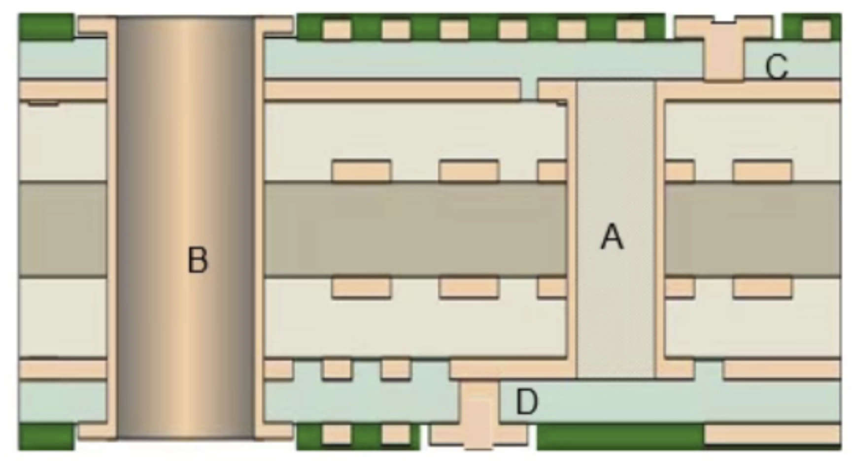
[Diagram: HDI Structure]
Note:
A = Buried Via,
B = Through Via,
C = Top Blind Via,
D = Bottom Blind Via.
1.3 HDI Process Flow Overview
HDI manufacturing processes are more complex than traditional PCBs, requiring handling of multiple key processes including laser micro-vias, buried vias, via plugging, and via filling plating.
Typical HDI Manufacturing Process:
- Panel Cutting/Material Preparation: Cut substrate according to production requirements
- Inner Layer Fabrication: Inner layer circuit imaging, etching, and inspection
- First Lamination: First lamination of inner layers with dielectric material
- Buried Drilling: Mechanical drilling to form buried vias
- Buried Plating/Plugging: Plating or resin plugging of buried vias
- Secondary Outer Layer Preparation: Pre-fabrication steps before outer layers
- Second Lamination: Second lamination process
- Laser Drilling: Create blind vias (Laser Via)
- Mechanical Drilling: Create through holes or larger diameter holes
- Via Filling Plating: Fill blind vias or required holes with copper
- Outer Layer Fabrication: Outer layer circuit imaging and etching
- Solder Mask: Solder mask ink coating and exposure
- Surface Finish (Optional): ENIG, immersion gold, immersion tin, etc.
- Routing/Profiling: CNC, V-Cut, edge milling, etc.
- Electrical Testing: Continuity and short circuit checking
- OSP (Optional): OSP coating if required
- Final Inspection: Appearance, dimensions, solder mask, hole diameter inspection
- Packaging & Storage: Storage after qualification
Note: Since HDI uses a cyclical process flow, each additional lamination, laser drilling, plating, and circuit step increases the technology level.
2. HDI Plating Process Purpose
After drilling (through holes) or laser drilling (blind vias) in HDI boards, the copper layers are separated by dielectric layers and cannot conduct.
Therefore required:
- Electroless Copper Deposition: Forms ultra-thin conductive layer on hole walls, providing conductive foundation
- Electroplating Copper Build-up: Fully metallizes holes, forming reliable conduction
Ultimately enabling stable, reliable electrical interconnection between all HDI layers.
3. HDI Plating Process Flow (Blind Via Board)
After blind via completion, pre-treatment, electroless copper deposition, panel plating, and via filling plating steps are required to form complete blind via conduction structure.
Process Flow:
-
Incoming from Previous Process
- Substrate after drilling/laser processing enters plating section
-
Deburring Line
- Remove hole wall burrs, resin, and drill smear
- (Equipment located in first-floor drilling workshop)
-
Baking/Plasma (Per MI Requirements)
- Clean hole walls and facilitate subsequent activation
-
PTH Horizontal Electroless Copper Line
- Deposit uniform conductive thin copper layer on hole walls
-
Blind Via Board Formation
- After electroless copper, forms blind via board ready for filling process
-
VCP Panel Plating (Flash Plating)
- Initial copper build-up to enhance subsequent filling capability
-
VCP Via Filling
- Use via filling plating solution to completely fill blind vias with copper
-
Inspection & Transfer to Next Process
- Check appearance, filling rate, and copper thickness before transferring to outer layer circuit process
4.2.1 Deburring - Sub-process Purpose
Main Functions
- Brush Wheel Removal of Surface Defects
- High-speed brushing to remove fingerprints, oxidation, drill burrs, and sharp edges
- High-Pressure Water Cleaning of Hole Contaminants
- Remove PP debris and dust to prevent hole blocking causing hole breakage defects
Deburring Line Process
- Automatic Panel Loading: Feed panels
- Scrubbing: Remove oxidation and burrs
- Water Rinse: Clean brushing residue
- High-Pressure Water Wash: Remove hole dust
- Drying: Dry internal/external moisture, prevent oxidation
- Automatic Panel Unloading: Complete panel collection
4.3.1 Plasma - Sub-process Purpose
Plasma treatment occurs in vacuum chambers, filled with specific gases like nitrogen, oxygen, CF₄, hydrogen, or argon, activated by RF electrodes to form plasma for treating board surfaces and hole walls:
Main Purposes
- Desmear
- Remove residual resin layers after drilling
- Activation
- Micro-etch material surfaces, improve adhesion, beneficial for electroless copper and plating
Baking Necessity
Generally requires pre-plasma baking to:
- Remove internal moisture from substrate
- Release stress
- Prevent delamination in subsequent processes or at customer end
To be continued!!
This is Part (1). The next installment will be released soon—stay tuned!
