Behind this lies the emergence of high-frequency, high-speed printed circuit boards (PCBs). They serve not only as physical carriers for chips but also as critical "highways" and "thermal foundations" ensuring successful overclocking. This article explores how PCBs meet the stringent demands of overclocking through advanced materials science, precision manufacturing processes, and hardware-software integration.
I. Overclocking: Performance Leap and Challenges
1.1 What is Overclocking?
Overclocking refers to the technique of manually adjusting hardware parameters (such as core voltage, multiplier, front-side bus frequency, etc.) to operate at frequencies beyond manufacturer-set safe values.
The principle lies in the fact that chip manufacturers typically set conservative rated frequencies to ensure mass production yield rates and stability. However, many chips with superior "physical quality" possess the potential to operate at higher frequencies when enhanced with better cooling and appropriate voltage increases.
Overclocking can significantly boost the performance of core components like CPUs, GPUs, and memory (RAM), delivering direct benefits such as increased frame rates (FPS) and reduced computation times, particularly in gaming, scientific computing, and data center applications.
1.2 Hardware Foundation and Challenges of Overclocking
Overclocking primarily targets two core hardware components:
2.1 Chips (CPU/GPU)
- These are the direct targets of overclocking
- Increasing frequency requires raising core voltage to maintain signal stability
- Power consumption and heat generation increase dramatically (Power ∝ Frequency × Voltage²)
- Chip "physical quality" and cooling solutions form the foundation of successful overclocking
2.2 PCB (Printed Circuit Board)
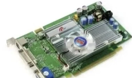
As the platform carrying all critical components including chips, power delivery modules, and memory particles, PCBs play the role of "unsung heroes" in overclocking.
Key Challenges:
II. High-Frequency PCB Materials: Foundation of Signal Transmission Highways
To address signal integrity challenges posed by overclocking, PCB material selection is crucial. Traditional FR-4 material exhibits excessive losses at high frequencies and can no longer meet requirements. High-frequency materials have become the preferred choice for overclocking PCBs due to their low dielectric constant (Dk) and low dissipation factor (Df) characteristics.
2.1 Critical Roles of Dk and Df
Low Dk/Dk Stability
- Dielectric constant (Dk) affects signal transmission speed in PCBs
- Low and stable Dk values ensure consistent signal transmission delay
- Reduces timing errors, crucial for precise signal synchronization at high frequencies
Low Df (Dissipation Factor)
- Key indicator measuring signal energy loss during transmission
- Lower Df means less signal attenuation and longer transmission distances
- Larger eye diagram opening and higher system stability
Material Comparison:
- Standard FR-4 (10GHz): Df ≈ 0.02
- PTFE (Polytetrafluoroethylene) substrate: Df ≈ 0.0013
- Rogers RO4350B: Df = 0.0037
- Panasonic Megtron series: Df ≈ 0.0017
2.2 Main High-Frequency Material Systems
PTFE (Polytetrafluoroethylene) Substrates
- Representative products: Rogers RO3003, Taconic TLY-5
- Characteristics: Df ≤ 0.002, excellent frequency stability
- Applications: Preferred for millimeter-wave (≥30GHz) applications
- Disadvantages: Difficult processing, high cost, poor adhesion
Hydrocarbon Resin (PCH)/Ceramic-Filled Modified Materials
- Representative products: Rogers RO4000 series, Shengyi S1000-2G
- Characteristics: Df < 0.0028, balanced performance, cost and manufacturability
- Applications: Servers and high-end graphics cards (GPU)
Polyphenylene Oxide (PPO) Substrates
- Representative products: Panasonic Megtron6/7
- Characteristics:
- Megtron6: Df ≈ 0.002
- Megtron7N: Df ≈ 0.0017
- Excellent conductive anodic filament (CAF) resistance
- Applications: HDI boards, data center server motherboards
2.3 Key Process Collaboration in PCB Manufacturing
Hybrid Lamination Technology
- Combination of high-frequency materials with standard FR-4
- Balances cost and performance
- Requires solving CTE matching and adhesion issues
- Uses plasma etching to enhance interface bonding
Low Roughness Copper Foil (VLP)
- High-frequency signals exhibit skin effect
- Uses rolled copper (Ra ≤ 0.3μm) instead of standard electrodeposited copper (Ra ≈ 1.5μm)
- Significantly reduces conductor losses and signal attenuation
Precision Impedance Control
- Impedance tolerance requirements within ±5% for overclocking
- Laser thickness gauges for precise dielectric thickness control
- Etching compensation technology (line width tolerance ±0.01mm)
- Comprehensive testing with network analyzers
Microvia and Routing Technology
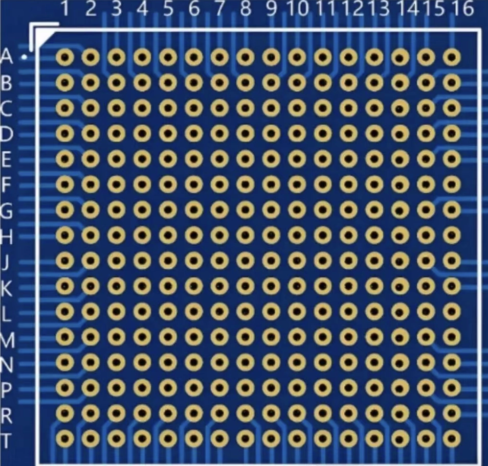
- Laser-processed micro blind vias (<0.1mm)
- Fine lines (line width/spacing ≤3mil)
- Routing principles: equal length, equal spacing, avoid right angles
III. Thermal Management: Foundation for Stable Overclocking
The massive power consumption from overclocking must be dissipated through effective cooling systems. PCBs undertake the dual task of conducting heat from both the chip core bottom and voltage regulator modules (VRM).
3.1 Thermal Management in PCB Materials
High Thermal Conductivity Materials
- Ceramic-filled hydrocarbon substrates: thermal conductivity ≥0.8W/m·K
- Special designs (embedded copper blocks, heat pipes): up to 5W/m·K
- Far superior to standard FR-4 materials
Heavy Copper Design
- Use thick copper foil (2oz, 3oz, 10oz) in power layers or thermal areas
- Utilizes copper's high thermal conductivity as built-in "heat spreaders"
- Rapid and uniform conduction of local hotspot heat
3.2 Thermal Optimization in PCB Structural Design
Thermal Via Arrays
- Dense arrangement of metallized vias under chip pads
- Configuration near power MOSFETs
- Rapid heat conduction from top layer to bottom or inner layer copper foil
Large-Area Copper Pouring and Thermal Pads
- Maximum copper pouring in non-routing areas
- Connection to ground networks to form thermal planes
- Thermal pads (Exposure Pad) connected via optimized via arrays
Composite Cooling Structures
- Copper substrate embedded heat pipes
- Direct integration of vapor chambers with PCBs
- Transforming PCBs into integral parts of cooling systems
IV. Hardware-Software Synergy: Intelligent Overclocking Closed Loop
4.1 Hardware-Level Coordination
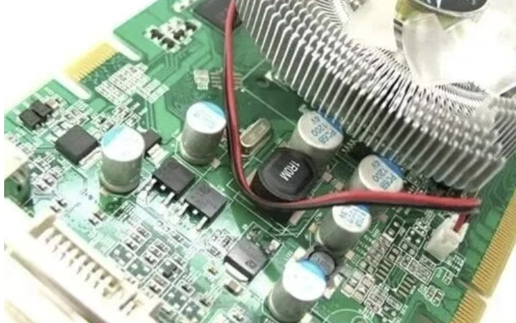
Precision Power Design (VRM)
- Multi-phase power design (e.g., 12+2 phases) in motherboards/GPUs
- High-quality DrMOS or GaN power components
- Solid capacitors for low ripple, high current power delivery
- Optimized power paths ensuring minimal voltage drop
Sensor Networks
- Distributed temperature, voltage, and current sensors on PCBs
- Real-time hardware status data acquisition
4.2 Software/Firmware-Level Coordination
BIOS/UEFI and Firmware
- User-friendly overclocking interface
- Adjustment of multipliers, voltages, memory timings, etc.
- Conversion of settings into hardware control commands
Dynamic Tuning and Protection
- Dynamic core frequency adjustment based on sensor feedback
- Automatic frequency reduction during overheating (Thermal Throttling)
Stability Testing Software
- Stress testing tools like Prime95, FurMark
- Verification of system stability after overclocking
Conclusion
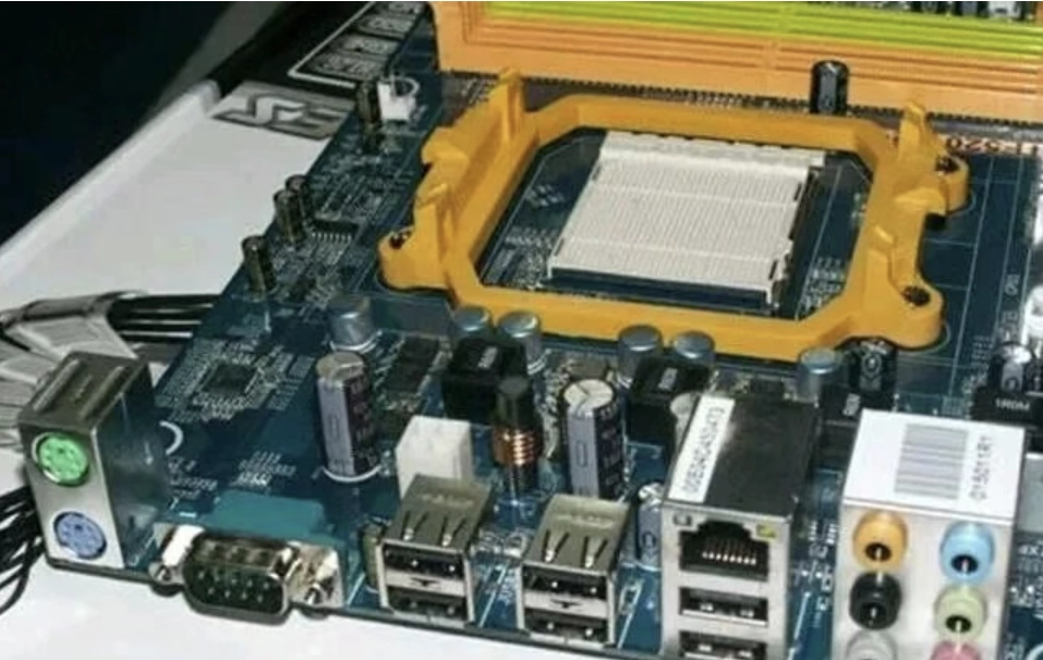
When first invented, printed circuit boards served merely conductive functions. However, in the world of extreme performance overclocking, PCBs have evolved from passive connection platforms into active participants integrating high-frequency signal transmission, high-current low-loss power delivery, and high-efficiency thermal management.
Through the adoption of low Dk/Df high-frequency materials, implementation of precision manufacturing processes (hybrid lamination, impedance control, microvia technology), optimization of thermal structural design, and deep integration with advanced power hardware, intelligent BIOS/UEFI firmware, and operating system software, modern PCBs pave the way for CPUs, GPUs, and other core chips to embark on their overclocking journeys with solid, stable, and efficient "highways" and "thermal channels."
