January 14, 2026
Focusing on the PCB prototyping and small-volume manufacturing needs of 2026, this article outlines four critical QA indicators that Layout Engineers must prioritize when selecting a PCB vendor: AOI, Flying Probe Testing, Impedance Control, and Cross-Section Analysis. It also explains how digital manufacturing platforms can solve issues related to opaque pricing and uncertain lead times. Discover how eCloud PCB utilizes cloud manufacturing to eliminate the "black box" of quoting and delivery anxiety.
In the electronics manufacturing landscape of 2026, for Layout Engineers, R&D personnel, and Mechatronics students in Taiwan, purchasing Printed Circuit Boards (PCBs) is no longer just a game of comparing prices. With the rising technical thresholds of 5G, IoT, and Edge Computing, the design complexity of circuit boards has increased exponentially.
Have you ever experienced this: Sending out your Gerber files only to have them disappear into a void? Receiving boards back only to find signal attenuation due to mismatched impedance? Or having a painstakingly designed prototype fail due to factory process errors?
Choosing the right PCB manufacturer is a strategic gamble involving Time-to-Market, Signal Integrity, and Long-term Reliability. This guide will take you out of the "manufacturing black box," using professional QA perspectives and digital trends to teach you how to select the most suitable PCB partner.
For a long time, a massive information gap has existed between PCB manufacturing and the Design House.
Engineers complete perfect DRC checks in EDA software (like Altium, KiCad), but once the files are sent to the factory via Email or FTP, they enter a "black box."
Traditional PCB quoting relies heavily on manual calculation by CAM engineers. A simple request for a double-sided board can take 1-3 business days. If there are Engineering Questions (EQ), both parties often communicate via forwarded Excel sheets through sales windows. Inconsistent terminology and communication gaps often lead to "talking past each other," or even result in erroneous design modifications.
The physical world is full of variables: etching causes undercut, and lamination leads to uneven resin flow. If a manufacturer lacks strong DFM pre-audit capabilities and fails to provide feedback on physical limitations before production, the final product often suffers from yield issues.
When selecting a PCB manufacturer, don't just look at their claimed "minimum trace width" or "highest layer count"; look at their "Verification Capability." High-quality PCBs are defined by testing. Here are four indispensable quality assurance links in modern PCB manufacturing:
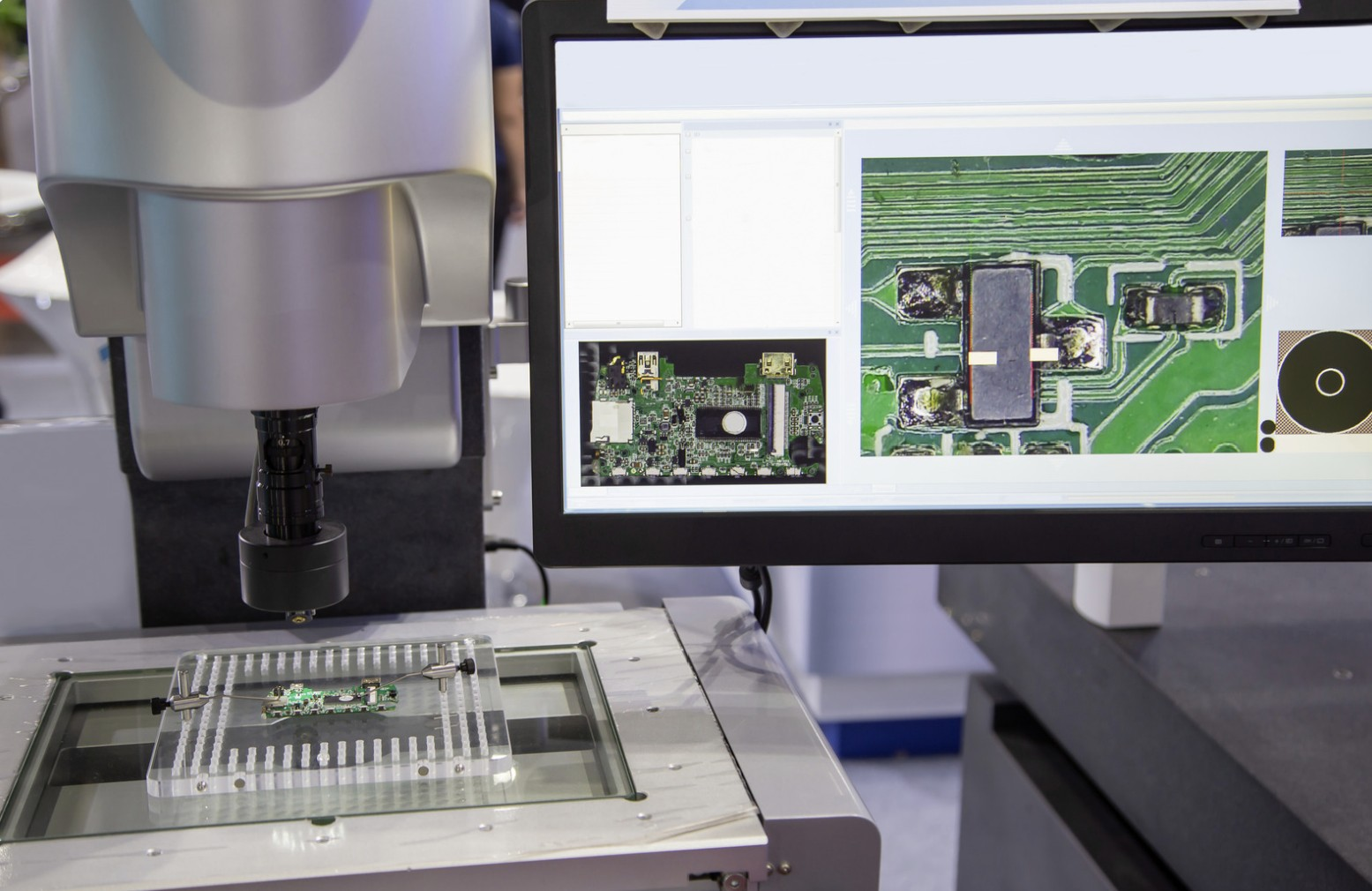
AOI is the first line of defense in PCB manufacturing. Modern high-end AOI systems use RGB structured light and algorithms to reconstruct the 3D contour of solder joints.
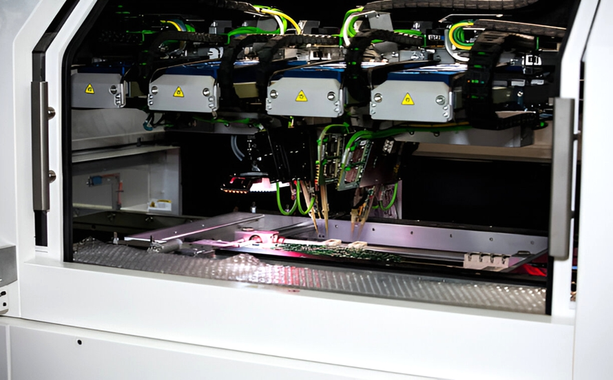
If AOI checks "appearance," Flying Probe Testing (FPT) checks the "nerves."
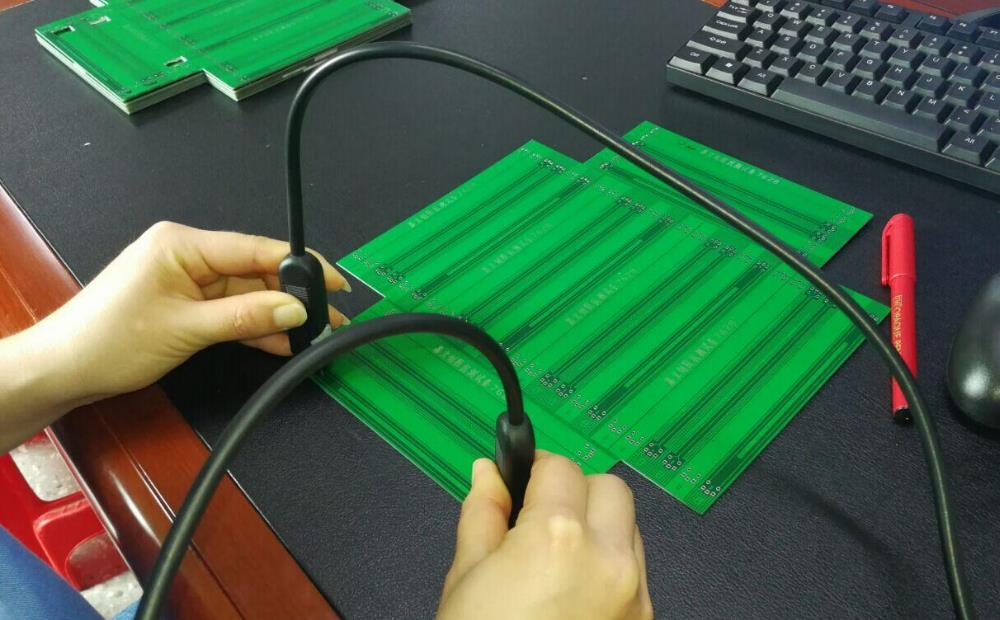
In USB 3.0, PCIe, DDR, or 5G antenna designs, the conductor is a transmission line. If the characteristic impedance (usually 50Ω or 100Ω) is discontinuous, it will cause signal reflection and data errors.
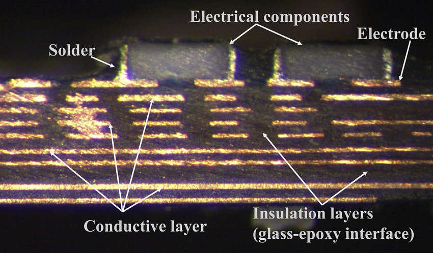
This is the ultimate method for verifying the internal structure of a PCB. It involves potting, grinding, polishing, and micro-etching a sample to observe the internal structure under a microscope.
After understanding professional QA standards, we find that eCloud PCB (逸雲科技) is precisely addressing the aforementioned pain points with its "Cloud-based, Digitalized" model, becoming a top choice for many Taiwanese engineers.
eCloud PCB has introduced a smart quoting engine. Users simply upload Gerber files, and the system automatically parses parameters.
Unlike contract manufacturers that only accept large orders, eCloud focuses on "Prototyping" and "Small Batches":
| Evaluation Dimension | Traditional PCB Factory | eCloud PCB | Value for Users | | :--- | :--- | :--- | :--- | | Quote Speed | Slow (1-3 days), manual calculation | Instant (< 1 min), automated algorithm | Rapid budget planning, accelerates development rhythm | | Transparency | Low (Black box), requires phone tracking | High (Visualized), real-time status updates | Accurate progress tracking, easier assembly planning | | MOQ | High, or expensive setup fees | Very Low (5-10 pcs), prototype friendly | Suitable for school projects, startup POC verification | | QA Inspection | Inconsistent standards, reports cost extra | Standardized (AOI/Flying Probe) | Ensures functional prototypes, reduces debug time |

Hardware innovation has no "Undo" button. A failed PCB prototype costs not just a few thousand NT dollars, but a precious week of iteration time.
As a professional Layout Engineer or R&D staff, you should establish a scientific supplier evaluation standard:
Ready to start your next project?
Visit the eCloud PCB official website now to experience the smooth process of transforming Gerber files into physical products. Your design deserves to be manufactured with high quality.
