Preface: When Apple "Backstabs" Jensen, The Show Begins
Fellow engineers, what has been the hottest topic in the pantries of Neihu and Hsinchu Science Park recently?
Aside from how many months of year-end bonus we're getting, it's probably the recent paper from Apple. They casually mentioned that their Apple Intelligence models were trained on Google TPUs, with absolutely zero mention of NVIDIA H100s. It’s like your friend with an iPhone suddenly declaring that the Pixel camera is superior—low damage, but extremely insulting.
In 2025, we stand at a pivotal turning point in computing history. For those of us at the core of Taiwan’s ICT industry—whether you are a Layout Engineer struggling with serpentine routing, a Thermal RD worrying about coolant leaks, or a testing brother at an OSAT validating CoWoS yields—this architecture war ignited by TPU vs. GPU is not just a spec upgrade. It is a fundamental redefinition of "computing."
Today, we won’t talk about ephemeral stock prices. We are going to de-cap the chips and go head-to-head with the technology, from the lowest level physical limits to your career development.
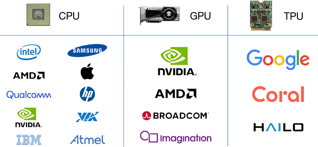
Chapter 1: The Architecture War — Brute Force vs. Precision Strike
Fresh graduates often ask me: "Senior, what exactly is the difference between a TPU and a GPU? Aren't they both just doing matrix math? Why did Google build their own?"
To understand this war, we must return to the "First Principles" of the bottom layer.
1. CPU: The Swiss Army Knife (General Purpose)
The design philosophy of a CPU is "Generality." A massive portion of its die area is dedicated to Control Logic and Cache to rapidly handle complex conditional branching (Branch Prediction).
- Engineer's View: It’s like a butler with a PhD. He can do anything, but if you ask him to move bricks (matrix multiplication), he thinks for three seconds before moving a single brick. Highly inefficient.
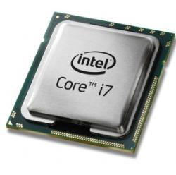
Source: Intel
2. GPU: The Chainsaw (Throughput Oriented)
NVIDIA’s GPU is essentially a SIMT (Single Instruction, Multiple Threads) architecture. It possesses thousands of small cores.
- Logic: It hides memory access latency through massive threading.
- Pros: High flexibility. Thanks to the invincible CUDA ecosystem, almost any custom kernel can run on it. This balance of generality and performance is why Jensen Huang has dominated AI for so long.
- Cons: To maintain this generality (supporting graphics rendering, scientific sim), GPUs retain a significant amount of Register Files and scheduling units. For pure matrix math, this is all Overhead.

Source: Nvidia
3. TPU: The Laser Cutter (Domain Specific)
Google's TPU (Tensor Processing Unit) is a thoroughbred ASIC. Its soul is the Systolic Array.
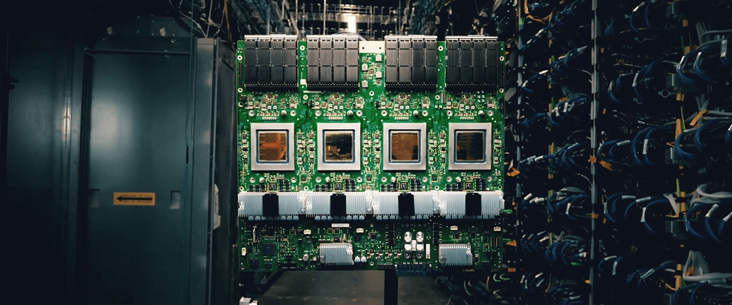
Source: Google
- What is a Systolic Array? Imagine data flowing like blood through vessels. In a GPU, data is frequently read from memory, calculated, and written back. In a TPU, Weights are pre-loaded and fixed in the compute units. Data (Activations) flows in from one end, washes over thousands of multipliers like a wave, and the result flows directly out the other end.
- Key Difference: Extreme Data Reuse. This drastically reduces memory access frequency, significantly lowering power consumption and increasing compute density. Google claims the 6th Gen TPU (Trillium) is over 67% more energy-efficient than its predecessor.
TL;DR: GPUs are born for "Parallelism"; TPUs are born for "Matrices."
Chapter 2: Hardware Limits — The Arms Race of Blackwell vs. Trillium
Let's get to the main event. What do the flagship monsters from these two camps look like in 2025?
1. NVIDIA Blackwell (B200/GB200): The Violence of Dual-Die
Jensen’s strategy is simple: Moore's Law is slowing down? Fine, I'll glue two chips together!
- Dual-Die Design: The B200 uses CoWoS-L packaging to stitch two full-reticle-limit GPU dies together, connected by a 10 TB/s NV-HBI link. To the software, it looks like a single super GPU with 192GB HBM3e.
- Power Nightmare: TDP has breached 1000W, heading towards 1200W. This is a massive challenge for board makers (like Gigabyte, MSI) and power supply vendors (Delta, Lite-On).
2. Google TPU v6 (Trillium): The Optical Counterattack of Vertical Integration
Google doesn't sell chips; they sell "Compute Service." This allows them to do insane things with their architecture.
- OCS (Optical Circuit Switching): This is Google's strongest moat. While NVIDIA clusters use copper (NVLink) or optical transceivers requiring expensive electrical-optical conversion, Google uses MEMS mirrors to dynamically adjust connections between TPUs purely in the optical domain.
- Advantage: If a rack fails, OCS can physically "bypass" it, reconfiguring the network topology in milliseconds. For training large models over months, this Reliability is priceless.
- Trillium Specs: TPU v6e delivers ~1836 TOPS (INT8). While single-chip raw power loses to B200 (9000 TOPS), TPU never fights 1v1. It fights in Pod Scale swarms.
Chapter 3: PCB & Signal Integrity — The Layout Engineer's Hell
This section is dedicated to Taiwan's Hardware RDs and Layout Engineers. If you thought PCIe Gen5 was a headache, AI Servers will make you question your life choices.
1. 224G SerDes: F1 Racing on Copper Foil
As signal rates move from 112G PAM4 to 224G PAM4, the tolerance for PCB materials and routing is practically zero.
- Material War: Panasonic Megtron 6 used to be high-end. Now, 224G designs basically demand Megtron 8 or AGC Meteorwave 8000 Ultra Low Loss materials.
- The Curse of the Via Stub: At 224G, a Via Stub acts like an antenna, causing severe Resonance. Current Design Rules require Stub Length to be < 6 mil (approx. 0.15mm).
- Backdrilling Limits: Taiwan's PCB houses (Unimicron, Gold Circuit Electronics) are forced to perform extreme precision backdrilling. Drill too deep, you cut the signal (Open); drill too shallow, the stub remains too long, and SI (Signal Integrity) fails immediately. This tests the absolute limits of manufacturing process capability.
2. Vertical Power Delivery (VPD): The Swiss Cheese PCB
To solve IR Drop and thermal loss caused by massive currents (1000A+) traversing the PCB, the trend is VPD.
- The Method: Power Modules (VRMs) are placed directly underneath the GPU/TPU (on the bottom side of the PCB), sending current vertically through the board to the chip.
- Layout Collapse: This means the area directly under the chip is riddled with Power Vias. Layout engineers must weave high-speed signal traces through these dense forests of power holes while managing Crosstalk. It is literally like carving art on a grain of rice.
Chapter 4: Thermal Revolution — Air is Dead, Long Live Liquid
In the face of 1000W, air cooling is officially dead. The GB200 NVL72 has made liquid cooling standard.
1. The Precision War of CDUs and Cold Plates
- Taiwan's Hidden Champions: I must name-drop the Taiwanese thermal giants here. Auras and AVC (Asia Vital Components) are transforming from module makers to System Integrators.
- Critical Component - UQD (Universal Quick Disconnect): This is the most unassuming yet lethal part of a liquid cooling system. One leak, and a multi-million dollar server rack is toast. Everyone is fighting for high-quality UQD capacity. Besides foreign players like Stäubli, Taiwan’s Fositek is aggressively entering this market.
2. The Google Way
Google's TPU Pods adopted liquid cooling very early. Their advantage is System-Level Optimization. Since they own the entire Data Center, they can design aggressive Cold Plates for TPU hotspots without worrying about standard server compatibility like NVIDIA does.
Chapter 5: Advanced Packaging — The Yield Rate Metaphysics of CoWoS
TSMC's CoWoS (Chip-on-Wafer-on-Substrate) is the physical foundation of all this, but it is also the bottleneck.
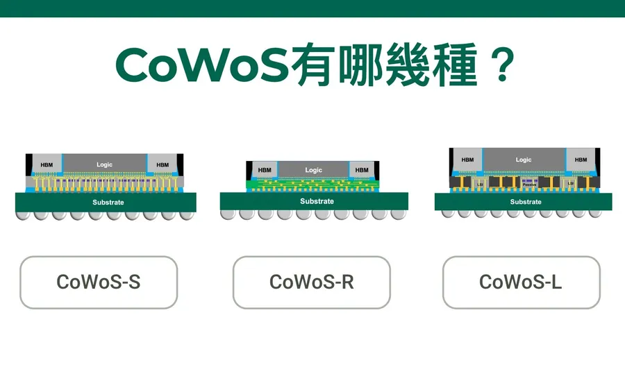
CoWoS-L vs. CoWoS-S
- CoWoS-S: Uses a full Silicon Interposer. High yield, but limited by Reticle Size. It can't get big enough.
- CoWoS-L: This is what Blackwell (GB200) uses. It utilizes an Organic Interposer combined with local LSI (Local Silicon Interconnect) bridges.
- The Challenge: Organic materials and Silicon have different CTEs (Coefficients of Thermal Expansion). Under high reflow temperatures, the package warps. This makes aligning the LSI Bridge notoriously difficult, which is rumored to be the main cause of Blackwell's early yield fluctuations.
- The Opportunity: This gives Taiwan's OSATs (ASE Holdings) and Test Interface vendors (WinWay, MPI) massive opportunities, as the demand for testing and debugging skyrockets.
Chapter 6: Software Tools — Who Can Break the CUDA Monopoly?
Hardware is just the ticket to enter; Software is the soul.
1. CUDA: NVIDIA's Absolute Defense
Developed over nearly 20 years, CUDA has created massive path dependency. Most researchers write PyTorch code that automatically interfaces with CUDA. This "ease of use" is NVIDIA's strongest moat.
2. JAX & Pallas: Google's Functional Counterattack
However, Google is tearing a hole in the fabric with JAX.
- JAX Advantage: Designed for the XLA compiler. On TPUs, JAX often outperforms PyTorch, especially in large-scale parallel training (SPMD).
- Pallas vs. Triton: For engineers seeking extreme performance, there is a new battleground.
- Triton (OpenAI): Allows you to write GPU Kernels in Python-like syntax, bypassing the high barrier of CUDA C++.
- Pallas (Google): An extension of JAX allowing you to write Kernels for TPUs, controlling data movement from HBM to VMEM. For Taiwanese Software RDs wanting to squeeze every drop of performance out of a TPU, this is a future prerequisite.
Chapter 7: Talent Market — Where is the Opportunity for Taiwanese Engineers?
Finally, what does this war mean for us in Taiwan?
1. Valuation Reset for System Makers (ODMs)
In the past, working on servers at Quanta, Wistron, or Inventec was seen as a stable but unexciting "14-month salary" job. That has changed.
- Who makes TPU Servers? It is an industry open secret that Google's TPU Servers are primarily manufactured by Inventec. Google has massive hardware R&D centers in Banqiao Tpark and Shilin, filled with projects collaborating with ODMs.
- Who makes NVIDIA GB200? Foxconn and Quanta have secured the major orders.
- Salary Structure: To snatch up talent who can handle Liquid Cooling and solve 224G SI issues, System Houses are now offering packages to Senior RDs that are very competitive, approaching Tier-2 IC Design house levels.
2. The Skill Tree: What to Upgrade?
- Hardware RD: Don't just draw schematics. Learn Signal Integrity (SI). Understand S-parameters and Transmission Line Theory. An SI engineer who understands 224G is a diamond in the rough right now.
- Thermal RD: Air cooling is history. Master Flotherm/Icepak for liquid cooling simulation. Understand fluid dynamics and CDU control logic. You won't go hungry for the next decade.
- Software RD: Don't just stick to CUDA. Play with JAX, understand Triton or Pallas. Future AI compute is heterogeneous; talent that understands optimization across multiple architectures is the scarcest resource.
Conclusion
The battle between TPU, GPU, and CPU likely won't have a single winner. The future is the era of Heterogeneous Computing. CPUs acts as the butler, GPUs handle the heavy general lifting, and TPUs manage massive matrix special ops.
For Taiwanese engineers, this is the worst of times (because the technical difficulty is enough to make you cry), and the best of times (because the whole world needs Taiwan's supply chain).
As long as the signals on our boards are clean, the water cooling doesn't leak, and the CoWoS yields pass, the arsenal of this AI revolution will continue to bear the mark "Made in Taiwan" or "Designed in Taiwan."
Everyone, keep grinding for Taiwan's semiconductor and system industries!
