##This report serves as a "Practical Summary," deeply analyzing process details from basic material physics to hybrid stack-ups. Combined with the latest dynamics from Taiwanese and global supply chains, it provides a comprehensive material selection combat guide for Taiwanese RDs and Mechatronics students. We will debunk myths and explore how to find that fleeting "Golden Balance" between pursuing extreme performance and controlling BOM costs.
Chapter 1: Material Physics and Economics—Breaking the FR-4 vs. High-Frequency Binary Opposition
In the past era of low speeds, PCB material selection was often a simple binary choice: use standard FR-4 (epoxy resin + glass fiber cloth) for the vast majority of cases, and consider expensive PTFE (such as the Rogers brand) only for a very small number of Radio Frequency (RF) designs. However, this dichotomy has completely failed in today's high-speed digital circuit design. As signal frequencies break through 10GHz, 20GHz, and even 100GHz, dielectric loss has become the main cause of signal attenuation, and the market has evolved a finely segmented spectrum of materials.
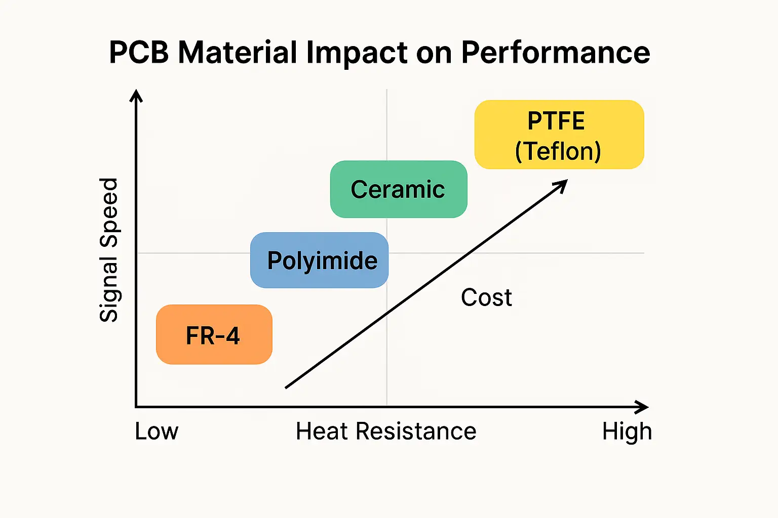
1.1 Deep Analysis of Frequency Response of Dielectric Constant (Dk) and Dissipation Factor (Df)
For senior RDs, Dk and Df are not just numbers on a datasheet; they represent the physical mechanisms of interaction between signals and materials at the microscopic level, as well as the associated cost implications.
1.1.1 Dk (Dielectric Constant): The Physical Meaning of Speed and Impedance
The dielectric constant (Dk) measures a material's ability to store electrical energy in an electric field.
- Signal Propagation Velocity: The speed of signal propagation Vp in PCB traces is inversely proportional to the square root of Dk. Low Dk materials mean faster transmission speeds, which is crucial for high-speed buses (like DDR5) that require strict timing budgets.
- Impedance Control and Trace Width: Given a fixed impedance (e.g., 50-ohm single-ended or 85-ohm differential), lowering Dk allows engineers to design wider trace widths. Wider traces mean a larger conductor cross-sectional area, thereby reducing the impact of "Conductor Loss" and the "Skin Effect".
- Cost Metaphor: Lowering Dk usually requires changing the resin formula (e.g., introducing PPE/PPO to replace epoxy resin) or using special low-Dk glass fabrics (like NE-glass), or even introducing hollow glass sphere fillers. These technical measures directly drive up material costs.
1.1.2 Df (Dissipation Factor): The Thermodynamics of Energy Loss
The dissipation factor (Df) represents the proportion of electric field energy converted into heat within the medium.
- Signal Attenuation: Df is the decisive factor in dielectric loss. At rates above 25Gbps, dielectric loss often exceeds conductor loss to become dominant. A change in Df from 0.020 (standard FR-4) to 0.002 (ultra-low loss material) can mean a signal improvement of over 10dB in a 20-inch long trace.
- Thermal Stability: Low Df materials usually also imply lower molecular polarity, which helps reduce the material's self-heating under high frequency and high power. This is particularly critical for OAM modules in AI servers that can consume hundreds of watts.
1.2 From Mid-Loss to Ultra Low-Loss: Material Grading and Cost Index
To balance performance and cost, RDs must be familiar with the characteristics and price ranges of materials at each grade. The following table synthesizes the performance and relative cost of mainstream market materials (based on standard FR-4 as 1.0):
| Grade | Dk @ 10GHz | Df @ 10GHz | Relative Cost (Cost Index) | Typical Applications | Representative Materials |
| :--- | :--- | :--- | :--- | :--- | :--- |
| Standard FR-4 | 4.2 - 4.5 | 0.015 - 0.020 | 1.0 | Consumer Electronics, IoT, Low-speed Control Boards | Nan Ya NP-175F, Isola 370HR |
| Mid-Loss | 3.8 - 4.0 | 0.010 - 0.015 | 1.3 - 1.6 | Entry Server, PCIe Gen 3 | Doosan DS-7409D, Shengyi S7045G |
| Low-Loss | 3.6 - 3.8 | 0.006 - 0.008 | 1.8 - 2.5 | Mainstream Server, PCIe Gen 4 | Panasonic Megtron 6, ITEQ IT-170GRA |
| Very Low-Loss | 3.4 - 3.6 | 0.004 - 0.005 | 2.5 - 3.5 | High-end Server, 100G Switch | ITEQ IT-968, EMC EM-888, Megtron 7 |
| Ultra Low-Loss | 3.2 - 3.4 | 0.002 - 0.003 | 4.0 - 6.0 | AI OAM/UBB, 400G/800G, PCIe Gen 5/6 | Megtron 8, EMC EM-892K, TUC ThunderClad 3+ |
| RF/PTFE | 2.9 - 3.2 | 0.001 - 0.002 | 8.0 - 15.0+ | 77GHz Radar, 5G Antenna | Rogers RO3003/4350B, Taconic TLY-5 |
Deep Analysis:
- The Price-Performance Trap: Many RDs are accustomed to using Panasonic Megtron 6 as a synonym for "high-end board material." However, in PCIe Gen 5 designs, Megtron 6's Df (approx. 0.004) may already be stretched thin, requiring expensive Retimer chips to compensate for the signal. At this point, if one upgrades to Megtron 7 or the Taiwanese equivalent EMC EM-891K, although the PCB cost rises, the Total BOM Cost may actually decrease if a Retimer can be saved. This is the essence of the "Golden Balance."
- The Extreme Cost of PTFE: While Rogers RO3000/4000 series have unbeatable electrical performance, their processing costs are extremely high (difficult to drill, requiring special plasma desmear). Unless it is for 77GHz radar or extremely high-frequency antennas, full-board use of PTFE should be avoided in digital circuits; this is the primary reason for the birth of "Hybrid Stack-up" technology.
1.3 Link Budget and the Mathematics of Material Selection
Material selection should not be based on feeling, but on a rigorous "Loss Budget."
Assume a PCIe Gen 5 channel (32 GT/s, Nyquist frequency 16 GHz) allows a total channel loss of -36 dB.
- Chip Package Loss: -4 dB
- Connector Loss: -2 dB
- Budget remaining for PCB traces: -30 dB
If the trace length is 15 inches:
- Using Mid-Loss material (loss approx. 1.2 dB/inch @ 16GHz): Total loss 18 dB -> PASS (Large margin).
- Using FR-4 (loss approx. 2.5 dB/inch @ 16GHz): Total loss 37.5 dB -> FAIL.
But if the trace length increases to 25 inches (like a large server backplane):
- Using Mid-Loss material: Total loss 30 dB -> Borderline PASS (High risk).
- Using Low-Loss material (loss approx. 0.9 dB/inch): Total loss 22.5 dB -> PASS (Safe).
The RD's job is to find the lowest-cost material grade that satisfies the Pass criteria through Simulation.
eCloud Suggestion for RDs 1
"Do not pay for excess performance, but do not let the PCB become the system bottleneck."
- Build your own loss database: Do not rely solely on vendor Datasheets. The real loss values under different stack-ups (Stripline vs Microstrip) and copper roughness (HVLP vs RTF) often differ from nominal values. It is recommended that RD teams build an internal database of measured material losses.
- System-level cost view (TCO): When evaluating material expense, include the cost of upgrading Retimers, Redrivers, and connectors. Sometimes, increasing PCB cost by $20 per square foot can save $50 in IC costs—this is true Cost Down.
- Leverage Taiwanese alternatives: Panasonic is the industry benchmark, but not the only choice. For non-core projects, materials from Elite Material (EMC), ITEQ, and Taiwan Union Technology (TUC) often offer better price-performance ratios and lead times.
Chapter 2: Core Design Logic of Hybrid Stack-up
When a single material cannot simultaneously meet electrical performance and mechanical strength requirements, or when using high-frequency material for the entire board is too costly, "Hybrid Stack-up" (or Hybrid Construction) becomes the solution. This technology has become mainstream in automotive radar, 5G antenna modules, and high-end server motherboards.

2.1 Physical Challenges of Hybrid Stack-up: The Curse of CTE Mismatch
The biggest headache in hybrid stack-up is the inconsistency in the Coefficient of Thermal Expansion (CTE) of different materials.
- CTE Mechanism: FR-4 is epoxy resin reinforced with glass fiber; its X-Y axis CTE is controlled by the glass fabric (approx. 12-16 ppm/°C), while the Z-axis CTE is controlled by the resin (larger). PTFE (like Rogers 3003) is a ceramic-filled fluoropolymer, and its CTE characteristics can be vastly different.
- Failure Modes:
- Delamination: When the board undergoes Reflow high temperatures (260°C), if the expansion rate difference between layers is too large, weak interfaces (usually between PTFE and FR-4 Prepreg) will tear apart.
- Via Barrel Crack: If the Z-axis CTE difference of the hybrid materials is large, the copper walls of the vias will be subjected to periodic tensile stress during thermal expansion and contraction, eventually leading to fracture and open circuits.
- Warpage: This is a nightmare for SMT processes. If the structure is asymmetric, the cooled board will curl like a potato chip, leading to BGA soldering failures.
2.2 Structural Symmetry: The First Iron Law of Hybrid Design
To combat the stress caused by CTE mismatch, the stack-up design must strictly adhere to "Symmetry."
- Material Symmetry: Using the center of the PCB as the axis, the material type, thickness, and resin content of the upper and lower layers must be as consistent as possible. For example, if the Top Layer uses 10mil Rogers 4350B, the Bottom Layer should ideally use the same material and thickness.
- Copper Distribution Symmetry: In addition to materials, the residual copper rate (Copper Balance) of each layer must also be balanced. RDs must lay "Dummy Copper" (Thieving) in empty areas during the Layout phase; this is not only for plating uniformity but also to balance thermal stress.
2.3 Selection Strategy for Bonding Systems
When laminating Rogers Core with FR-4, ordinary FR-4 Prepreg sometimes cannot provide enough bonding force, or its flow characteristics (Rheology) cannot fill the micro-pores on the Rogers surface.
- Compatible Prepreg: Rogers 4000 series are hydrocarbon ceramic materials, intentionally designed to have processing characteristics close to FR-4, so standard High-Tg FR-4 Prepreg (like Isola 370HR PP) can usually be used directly.
- Dedicated Bonding Films (Bondply): For pure PTFE materials (like Rogers 3000), dedicated Bondply (like RO3001 or 2929 Bondply) or Anisotropic Conductive Film (ACF) type materials are usually required. These provide better chemical bonding but are more expensive and have a narrower processing window.
- Process Sequence: A common practice is "Cap Construction"—the FR-4 inner layers are fabricated with circuitry first, and then the Rogers Core is laminated on the outermost layer. This protects the fragile high-frequency material from excessive process damage.
2.4 Practical Case: Hybrid Structure of Automotive 77GHz Radar
Automotive radar requires extremely low-loss PTFE material (like Rogers RO3003, Dk=3.0, Df=0.0010), but using RO3003 for the entire board is too expensive and mechanically too soft.
- Solution:
- L1-L2 (RF Layer): Use 5mil or 10mil Rogers RO3003. RF signals travel on L1 microstrip lines with L2 as reference.
- L2-L3 (Bonding): Use FR-4 Prepreg (must be Low Flow or dedicated Bondply) for bonding.
- L3-L6 (Digital/Power): Use High-Tg FR-4 Core (like ITEQ IT-180 or Nan Ya NP-175F). Digital control signals and power run on these cheap and sturdy layers.
- Advantages: Critical millimeter-wave signals transmit entirely on high-performance material, while the digital part uses cheap material, and the FR-4 provides the necessary mechanical stiffness for the whole board, facilitating installation and heat dissipation.
eCloud Suggestion for RDs 2
"Hybrid stack-up is an art; symmetry is its soul."
- Early Vendor Involvement: Do not wait until the Layout is finished to ask the factory if they can make it. Hybrid Stack-up requires special lamination parameters (ramp-up rate, pressure profile). Be sure to request "Verified Hybrid Reference Stack-ups" from Nan Ya, Unimicron, or Unitech early in the design phase.
- Focus on Z-axis CTE: When selecting FR-4 materials to mix with Rogers, be sure to choose models with High-Tg (Tg > 170°C) and Low Z-CTE. This minimizes Z-axis stretching during thermal cycling and protects vias.
- Avoid "Island" Effects: In the FR-4 layer regions of a hybrid board, large areas of copper foil help grip the resin and reduce the risk of delamination. Do not leave large areas without copper at the interface.
Chapter 3: The Rise of the Taiwanese Supply Chain—Cost-Performance Alternatives
Historically, the high-end high-frequency material market was dominated by American (Rogers, Isola) and Japanese (Panasonic, Mitsubishi) manufacturers. However, in recent years, with the explosion of AI server demand and geopolitical supply chain restructuring, Taiwanese local material manufacturers have made huge technological breakthroughs, offering highly competitive alternatives. This is an important weapon for RDs to control costs.
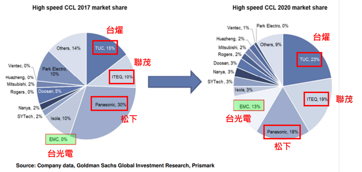
3.1 The Counterattack of ITEQ and EMC
In NVIDIA's AI server and Google TPU supply chains, Taiwanese material manufacturers are no longer supporting actors but core suppliers.
3.1.1 Elite Material Co. (EMC)
- Strength: Dominator of Halogen-free materials, with a very high market share in mobile phones and handheld devices, and significant gains in the AI Server field in recent years.
- Killer Product: EM-892K / EM-892K2. Positioned as Ultra Low Loss, primarily targeting Panasonic Megtron 7/8. Its Df value can reach below 0.002 (@10GHz), and it has excellent heat resistance, already widely used in 800G switches and high-end AI server motherboards (UBB).
- Application Advice: If the project requires strict environmental compliance and pursues extreme performance, EMC is the top choice.
3.1.2 ITEQ Corporation
- Strength: Long-term cultivation in networking and server infrastructure, with a product line covering Mid-Loss to Extreme Low Loss.
- Killer Product: IT-968 / IT-988GSE. IT-968 is currently the king of cost-performance in the server market, with performance close to Megtron 7 but at a more advantageous price. Its special resin formula gives it excellent Dk stability after multilayer lamination.
- Application Advice: For PCIe Gen 5 servers or 400G switches, IT-968 is a choice that can significantly reduce costs while providing sufficient performance.
3.2 Taiwan Union Technology (TUC) and Nan Ya Plastics
3.2.1 Taiwan Union Technology (TUC)
- Strength: Known as the "Invisible Champion," with deep technology in the ultra-low loss material field.
- Killer Product: ThunderClad 3+ (TU-933+). Designed specifically for 112G/224G applications, it is extremely competitive in electrical performance and excels in thermal reliability, suitable for High Layer Count backplane designs. Its special Hyper Very Low Profile (HVLP) copper foil bonding technology makes its high-speed signal performance comparable to major Japanese manufacturers.
- Application Advice: When encountering extremely high layer counts (>30 layers) in backplane design and worrying about CAF issues, TUC's materials are worth evaluating.
3.2.2 Nan Ya Plastics
- Strength: Vertical integration capabilities of the Formosa Plastics Group (glass yarn, copper foil, resin all made in-house), unrivaled cost control capabilities.
- Killer Product: NP-175F / NP-175F (Low Loss). Although Nan Ya started later in the Ultra Low Loss field, it is the absolute king in Mid-Loss and High-Tg FR-4 fields. NP-175F has extremely stable quality and is often used as the "non-signal layer" in Hybrid boards to reduce costs.
- Application Advice: In hybrid stack-up designs, using NP-175F as Core and Prepreg for power and ground layers, combined with high-end materials for outer layers, is the best combination to lower BOM Cost.
3.3 Key Indicators for Qualifying Second Sources
When RDs want to introduce Taiwanese materials to replace Japanese/American materials for cost reduction, they cannot look only at Dk/Df on the Datasheet. Strict validation processes must be executed:
- CAF (Conductive Anodic Filament) Tolerance Test: AI servers typically operate at high voltages (48V/54V) with minimal layer-to-layer spacing. Materials must pass Temperature Humidity Bias (THB) testing to ensure copper filaments do not grow and cause internal shorts.
- Moisture Absorption: Water absorption is the invisible killer of PCBs, causing Dk/Df to rise (water is a high-Dk substance) and triggering popcorn effects during reflow. Taiwanese materials have significantly reduced moisture absorption after formula improvements, but one still needs to watch the water absorption data in the Datasheet (typically should be < 0.1%).
- Surface Roughness: Material vendors usually offer multiple copper foil options (Standard, RTF, VLP, HVLP). Sometimes, using a cheaper dielectric material paired with HVLP (Hyper Very Low Profile) copper foil can yield signal performance superior to an expensive dielectric paired with standard copper, at a lower cost. This is a frequently overlooked Cost-down technique.
eCloud Suggestion for RDs 3
"Leverage supply chain competition and build a tiered AVL."
- Build a tiered AVL (Approved Vendor List): Do not list just one part number on the BOM.
- Tier 1 (Core Signal Layers): Specify Panasonic Megtron 7 or EMC EM-892K (Ensure Performance).
- Tier 2 (Secondary Power Layers): Open to Nan Ya NP-175F or ITEQ IT-180 (Ensure Cost).
- HVLP copper is a low-cost upgrade artifact: If your simulation results show losses are Marginal, don't rush to switch to more expensive resin materials. Try asking the vendor: "Can this material be paired with HVLP copper?" Usually, the loss improvement from HVLP (reducing skin effect) is very significant, while the cost increase is far less than upgrading the resin.
- Focus on vertically integrated vendors: Manufacturers like Nan Ya who make their own glass fabric and copper foil usually offer better supply stability and price fluctuation control during capacity crunches (like AI booms) compared to pure laminators.
Chapter 4: Practical Case Analysis of AI Servers and High-Speed Computing
AI servers represented by NVIDIA H100/H200 or GB200 are the pinnacle of current PCB technology and the best examples of hybrid stack-up and high-end material application. Understanding the material selection logic of these top-tier products gives RDs a broader perspective when designing mid-to-low-end products.
4.1 OAM (OCP Accelerator Module) Material Selection Strategy
OAM modules (like NVIDIA's GPU modules) carry core computing chips, with extremely high signal rates (112G PAM4) and huge current density.
- Design Features: Typically 18-24 layers, high-density HDI (3-stage or 4-stage Any-layer), extremely high routing density.
- Material Selection:
- Performance First: Must use Ultra Low Loss materials (like Megtron 8, EMC EM-892K, TUC ThunderClad 3+). Because in such a small space, heat dissipation and signal integrity are absolute bottlenecks with no room for compromise.
- Hybrid Strategy: OAMs rarely use hybrid stack-up. Why? Because OAMs are small, have many layers, and many blind/buried vias; mixing materials with different CTEs would lead to extremely high HDI process risks (laser drilling misalignment, hole wall separation). Furthermore, the OAM unit price is extremely high (thousands of dollars), so the PCB material cost is relatively small, favoring full-board use of top-tier materials to ensure reliability.
4.2 Hybrid Design of UBB (Universal Baseboard)
UBB is the large-sized mainboard carrying 8 OAMs, huge in size (usually larger than 20x24 inches) and high in layer count (22-26 layers).
- Design Features: Super large size, long-distance routing (must span the entire board to connect GPUs), massive power requirements (thousands of watts).
- Material Selection and Hybrid Practice: UBB is a typical application scenario for hybrid stack-up.
- High-Speed Signal Layers: Use Megtron 7/8 grade materials to ensure 112G/224G signal quality between GPU-GPU and GPU-Switch.
- Power/Ground Layers (Middle Layers): Since UBB needs huge current transmission capability, the middle thick copper layers (2oz/3oz) are mainly responsible for conduction and heat dissipation, and are insensitive to Dk/Df. Therefore, High-Tg FR-4 (like Nan Ya NP-175F) or Mid-Loss materials can be used here.
- Economic Benefit: A UBB area is huge; if the entire board uses Megtron 8, the cost would be astronomical. By replacing the middle 10-14 layers with FR-4, material costs can be reduced by 30%-40%, and the better mechanical rigidity (Young's Modulus) of FR-4 helps suppress sagging and warpage of the large board during Reflow.
4.3 Glass Core Substrates and Future CPO Trends
Although not yet widespread, for next-generation Co-Packaged Optics (CPO) and 224G/1.6T transmission, traditional organic materials (Organic Substrate) are approaching their limits.
- Glass Substrate Advantages: Glass has extremely low Dk/Df and is extremely flat (Roughness near zero), perfectly supporting fine line (<5um) lithography processes. More importantly, the CTE of glass can be adjusted to match Silicon Dies completely, solving thermal stress issues.
- RD's Foresight: Although still in the R&D stage, understanding TGV (Through Glass Via) technology and glass substrate characteristics helps RDs plan technical roadmaps for the next 3-5 years.
eCloud Suggestion for RDs 4
"Hybrid for Big Boards, Full High-End for Small Boards."
- Size determines strategy: For small-sized, high-density, high-value modules like OAM, do not try to save pennies with hybrid stack-up; the HDI yield risk will outweigh the gains.
- Large UBB-class boards must hybridize: For server motherboards or backplanes, hybrid stack-up is almost mandatory. But note that the FR-4 part of the hybrid must be a "Low Flow" model or one compatible with high-frequency materials to avoid uneven resin flow during lamination leading to uncontrolled thickness and impedance.
- Learn from Reference Designs, but Validate: NVIDIA or Intel Reference Designs usually specify the highest-spec materials to ensure a Pass. But in the mass production phase, the RD's value lies in finding Cost-down space through validation (e.g., introducing Taiwanese hybrid materials on UBB).
Chapter 5: Advanced Manufacturing and Cost Control—What Else Besides Material Unit Price?
Many RDs, when estimating BOM costs, only calculate the unit price of each Core and Prepreg, ignoring "Hidden Costs." In hybrid stack-up, hidden costs often account for more than 30% of the total cost.
5.1 Costs of Process Complexity (Process Overhead)
- Lamination Cycles: Standard Through Hole boards require only one lamination. But if 2-stage or 3-stage HDI (like 3+N+3) is designed, or Buried Vias are needed, it requires 2, 3, or even more lamination cycles. Each cycle implies factory capacity usage, energy consumption, and yield risk.
- RD Strategy: Without compromising routing density, try to minimize HDI stages. For example, by optimizing Fan-out design, simplifying 3+N+3 to 2+N+2 often saves more cost than changing materials.
- Drilling Costs (Laser vs. Mechanical):
- Mechanical Drilling: PTFE material is soft and tough, easily clogging drill bits and creating smear. The life of a drill bit drilling PTFE may be only 1/3 of that drilling FR-4, and special feed parameters are needed.
- Laser Drilling: For glass-fiber-containing high-frequency materials, laser ablation efficiency is lower, and hole shapes tend to be tapered, affecting plating quality.
- Desmear: High-frequency materials are chemically inert; traditional permanganate desmear is ineffective, usually requiring expensive Plasma cleaning processes. This is one reason for the high cost of hybrid boards.
5.2 Yield Loss and Panel Utilization
- Panel Utilization: This is the most direct but most overlooked cost. PCBs are produced on standard-sized "Working Panels" (e.g., 18x24, 21x24 inches).
- Case: Suppose your single board size is designed as 200mm x 150mm; utilization might be 85%. But if you arbitrarily increase it to 210mm x 160mm, it might cause one less piece per panel, dropping utilization instantly to 60%. This means you wasted 40% of expensive high-frequency material.
- Registration: In hybrid stack-up, different materials have different scaling factors, making inner layer alignment extremely difficult. The more layers, the severe the accumulated alignment deviation, leading to via breakout or open circuits, which is the main cause of scrap in hybrid boards.
5.3 Hidden Costs of Impedance Control
In hybrid stack-up, impedance calculation becomes very complex due to the use of materials from different vendors with different Dk. If RDs rely only on software simulation without considering the factory's actual "Press-out Thickness," the produced boards may fail impedance specs, leading to batch scrap.
- Prepreg Flow Thinning: In high-resin-content Low-loss PP, the thickness after lamination will be thinner than the nominal value. RDs must use the "Post-Press Thickness" provided by the PCB factory to calculate impedance, not the original thickness on the Datasheet.
eCloud Suggestion for RDs 5
"Cost is not negotiated by procurement; it is designed by RDs."
- Ask about Panelization before sizing: Before the ME Stack-up is finalized, take the estimated size to the PCB factory and ask: "What is the utilization rate of this size on your working panel?" Sometimes, shrinking length and width by just 2mm can increase utilization by 15%, which is a direct 15% discount.
- Reduce unnecessary vias: Blind/buried vias are useful but are cost killers. Optimizing layout to replace some blind vias with through holes, or reducing the number of Back-drills, can significantly lower processing costs.
- DfM (Design for Manufacturing) is mandatory: Don't just draw circuits. Understand the principles of plasma desmear, the limits of laser drilling, and lamination tolerances. An RD who understands the process designs boards that not only perform well but are also favored by factories with high yield—this is the true "Golden Balance."
Conclusion
In the electronic design race of 2025 and beyond, "Performance" and "Cost" are no longer mutually exclusive options but boundary conditions that must be met simultaneously. For Taiwanese RD engineers, mastering the physical nature of materials, becoming proficient in hybrid stack-up processes, and familiarizing themselves with the advantages of the Taiwanese supply chain are key to advancing from a mere "Executor" to a "System Architect."
We need not blindly worship expensive imported materials, nor fear the risks of hybrid stack-up. Through precise link budget analysis, symmetrical structural design, and deep collaboration with the supply chain, we are fully capable of designing golden products that meet the stringent performance requirements of the AI era while possessing extreme cost competitiveness. This is not just a victory for technology, but a manifestation of Taiwan's R&D value.
