January 12, 2026
In the current global semiconductor and electronic component supply chain, Taiwan consistently plays a pivotal role in core technology output. With the leapfrog developments in Artificial Intelligence (AI), Low Earth Orbit (LEO) satellite communications, and High-Performance Computing (HPC), the Printed Circuit Board (PCB)—often called the "Mother of the Electronics Industry"—is a critical factor. The efficiency and quality of the PCB R&D stage directly determine a product's time-to-market advantage.
PCB Prototyping refers to specialized manufacturing services catering to low-volume, diverse, and experimental requirements during the early stages of R&D. The core objective is to verify Layout accuracy, Signal Integrity (SI), and Power Integrity (PI).
In the Taiwanese industrial context, the term "Quick-turn" (快洗) has a unique historical background. Originally, it referred to the rapid production of single or double-sided boards in labs or small workshops using simple chemical etching equipment. However, as packaging technologies evolved toward BGA (Ball Grid Array), 0201 components, and even smaller form factors, modern "Quick-turn" has evolved into a highly automated, high-precision service capable of manufacturing complex Multi-layer Boards within extremely tight lead times.
For professional service platforms like ecloudpcb.com, understanding the differentiated needs between prototyping and quick-turn is essential:
According to 2024 data for the Taiwan PCB industry, annual output value reached NT$816.8 billion, with the most significant growth in high-end HDI (High-Density Interconnect) boards. This reflects a shift in R&D demand from traditional through-hole technology to micro-via and blind/buried via technologies.

The Taiwan PCB industry showed signs of recovery in Q4 2024, with quarterly output reaching NT$217.5 billion. This growth is primarily driven by three sectors: AI Servers, Satellite Communications, and Automotive Electronics. For R&D engineers, this necessitates designing for higher signal frequencies and more rigorous thermal environments.
| Industry Segment | 2024 Growth Rate | Primary Drivers | | :--- | :--- | :--- | | High-end HDI | 10.7% | AI computing modules, satellite antennas, high-performance mobile devices. | | Substrate | Steady Recovery | High-Performance Computing (HPC) chip packaging. | | Traditional Multi-layer | 2.8% | Industrial control systems, general-purpose servers. | | Flexible PCB (FPC) | 4.5% | Wearable devices, automotive displays, and sensor modules. |
Understanding the PCB manufacturing flow is a fundamental skill for every R&D engineer.
Image transfer moves the circuit pattern from EDA software to the copper-clad laminate. To shorten lead times, many quick-turn factories now utilize LDI (Laser Direct Imaging). This replaces traditional phototools (film), improving alignment accuracy and eliminating errors caused by film distortion due to humidity.
During Dry Film Lamination, the board surface must undergo thorough cleaning and micro-etching to ensure adhesion. Improper pre-treatment leads to "Open" or "Short" circuits during etching. For fine lines below 4mil (approx. 0.1mm), cleanroom environments and precise exposure energy control are vital.
Vias are essential for interlayer connectivity. The PTH (Plating Through Hole) process involves two core steps: Desmear and Electroless Copper. Desmear uses strong oxidants to remove resin residue (smear) caused by drill friction, ensuring a solid ohmic contact between the hole wall and internal copper layers.
Etching determines the final width of the circuit traces. Due to the "Undercut" phenomenon, engineers must account for Etch Compensation. If a design requires a 5mil line width, the factory may compensate the film to 5.5mil to offset the loss during chemical etching.
Proficiency in Altium Designer, KiCad, or Allegro is a prerequisite for R&D engineers and students. However, most design failures occur during the file output phase.
For the widely used Altium Designer, a correct output includes Gerber Files and NC Drill Files:
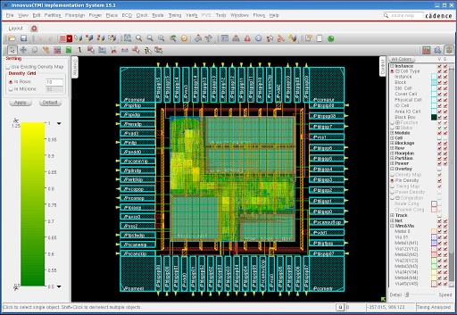
| EDA Term | Physical Meaning | R&D Note | | :--- | :--- | :--- | | Top/Bottom Layer | Copper traces. | Check current capacity and voltage drop. | | Solder Mask | "Green oil" insulation. | A "negative" layer; openings indicate exposed copper. | | Silkscreen | White text/legends. | Avoid pads to prevent soldering issues. | | Keep-out Layer | Routing boundary. | Defines the board outline or internal cutouts. | | Internal Plane | Reference planes. | Used for GND or VCC for stability and shielding. |
For budget-sensitive students and startups, understanding the pricing logic is key. In Taiwan, the "Basic Engineering Fee + Per-piece Fee" or "Promotional Bundle" models are standard.
Modern R&D requires more than just bare boards. Turn-key services—integrating component sourcing and SMT (Surface Mount Technology)—are becoming the mainstream. This allows engineers to outsource tedious soldering and focus on software debugging.
Students from major universities (NTU, NYCU, NTHU, NCKU, etc.) are vital users of the prototyping market. Their specific needs include:
ecloudpcb.com should address these pain points with dedicated "Student Discount Zones" and precision marketing through social media platforms like Facebook electronics groups and Dcard university boards.
The industry faces unprecedented shifts. AI servers require massive power, making Thermal Management a priority. The use of Embedded Copper Coins and Heavy Copper technology in the prototyping stage is increasing. Furthermore, global regulations like RoHS 2.0 and REACH mandate lead-free processes (Lead-free HASL) and eco-friendly substrates—not just for CSR, but as a "passport" to the international supply chain.
PCB prototyping is evolving from a "manufacturing industry" into a "technical service industry." Through digital integration on platforms like www.ecloudpcb.com, engineers and students can innovate faster and at a lower cost. In an era of intense global tech competition, mastering PCB prototyping and market resources is the key to maintaining Taiwan's leadership in the electronics sector.
