When discussing the electrical performance of high-speed PCBs, four key terms are absolutely essential: dielectric constant (Dk), loss tangent (Df), characteristic impedance (Z0), and insertion loss (IL). These factors are interrelated and collectively determine the quality of signal transmission on the circuit board. Today, let’s take a deep dive into these “Big Four”!
I. Definitions and Physical Significance of the Four Key Parameters
1. Dielectric Constant (Dk / εr): The "Speed Bump" for Signals
The dielectric constant is a physical quantity that measures a material's ability to store electrical energy under an electric field. Simply put, it reflects the degree of "resistance" a signal encounters when propagating through the medium. It is a dimensionless relative value.
- Numerical Significance: Common FR-4 laminates have a Dk between approximately 4.2 and 4.8, while high-frequency materials like PTFE (Teflon) typically range from 2.2 to 3.0. The lower and more stable the Dk value, the faster the signal propagation speed, which is more favorable for high-frequency transmission.
2. Dissipation Factor (Df / tan δ): The "Thief" of Energy
The dissipation factor (also known as loss tangent or dielectric loss tangent) is a parameter that characterizes the energy loss in a material due to polarization lag effects under an alternating electric field. It represents the ratio of the portion of signal energy "lost" to the insulating laminate compared to the energy stored within the material.
- Numerical Significance: The smaller the Df value, the better. Ordinary FR-4 has a Df around 0.02, while high-frequency, high-speed materials (such as Rogers RO4350B) can be as low as 0.0037 or even lower. The smaller the Df, the less signal heating and attenuation caused by the material itself.

3. Characteristic Impedance (Z0): The "ID Card" of a Transmission Line
Characteristic impedance is the ratio of instantaneous voltage to instantaneous current encountered by a signal propagating along a transmission line, measured in Ohms (Ω). It is not simply DC resistance but is determined by the distributed resistance (R), inductance (L), conductance (G), and capacitance (C). At high frequencies, it can be approximated as Z0 = √(L/C).
- Numerical Significance: In PCB design, common single-ended signal line impedance targets are 50Ω or 75Ω, while differential signals are typically 90Ω or 100Ω. Maintaining impedance continuity (impedance matching) is absolutely critical to preventing signal reflections.
4. Insertion Loss (IL): The "Toll" for Signals
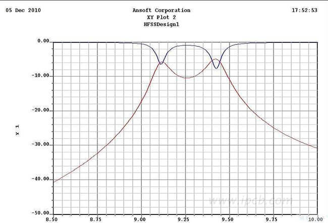
Insertion loss refers to the attenuation of power at the output end of a transmission line relative to the input end, typically expressed in decibels (dB). Its mathematical definition is S21 = -10 * log(Po/Pi).
- Unit Clarification (dB/inch vs. dB):
- Material Context (dB/inch): For standardization, material suppliers normalize insertion loss per unit length (commonly dB/inch in the US, dB/cm in Asia). This reflects the "loss characteristic of the material itself."
- System Context (dB): When a Layout engineer calculates the total attenuation for an actual trace (e.g., a 10-inch trace), the resulting total insertion loss does not have a length unit, as it is the total attenuation value for that specific path.
II. Interrelation of the Four Key Parameters: From Material to Final Performance
These four parameters do not exist in isolation; they form a complete chain of cause and effect:
- Dk Determines Impedance, Impedance Affects Matching: The value of characteristic impedance depends heavily on Dk. According to the microstrip formula Z0 = [87 / √(εr + 1.41)] × ln[5.98H / (0.8W+T)], if the Dk of the laminate fluctuates significantly, the actual impedance will deviate from the design value, leading to signal reflections and degraded Signal Integrity (SI).
- Df and Dk Together Determine Dielectric Loss: The dielectric loss formula is αd ∝ f × tan δ × √εr. The higher the frequency, the more significant the impact of Df and Dk on insertion loss.
- Impedance Accuracy Directly Affects Insertion Loss Testing: Before measuring insertion loss with a Vector Network Analyzer (VNA), impedance matching must be ensured. If impedance is mismatched, the measured "loss" will include a significant amount of energy lost due to reflections, leading you to mistakenly believe the material's Df is poor.
- The Hidden Culprit—Copper Foil Roughness: To achieve low loss at high frequencies, the Dk/Df of laminates have been pushed to extremes. However, due to the Skin Effect, high-frequency currents travel along the surface of the copper foil. If the copper surface is too rough, the transmission path lengthens, and conductor loss increases dramatically. Therefore, high-speed boards must use low-roughness copper foils (such as RTF or VLP copper).
III. Debunking Common Myths: How Trace Width and Spacing Affect Impedance and Insertion Loss
Many engineers often confuse the "rules for impedance" with the "rules for insertion loss." Let's clarify this once and for all:
1. Regarding Differential Impedance
- Wider Trace Width (W) → Lower Impedance (✅) : Increasing trace width increases the capacitance (C) to ground. According to Z0 = √(L/C), impedance decreases.
- Larger Spacing (S) → Higher Impedance (✅) : Increasing the spacing between two lines weakens their mutual coupling capacitance, making them behave more like independent single-ended lines, thus increasing the differential impedance.
2. Regarding Insertion Loss
- Wider Trace Width (W) → Lower Insertion Loss (✅) : Wider traces have a larger conductor cross-sectional area, reducing DC resistance and effectively reducing conductor loss, resulting in better insertion loss performance.
- Larger Spacing (S) → No Change in Insertion Loss (✅) : Spacing has a negligible effect on the inherent loss of a single trace. In other words, the rules for impedance ≠ the rules for insertion loss! Insertion loss (related to resistance/energy dissipation) and spacing (related to reactance/coupling) are decoupled.
IV. Advanced Discussion: Does Insertion Loss Distinguish Between "Single-Ended" and "Differential"?
This is a very precise engineering question.
- At the Physical Level: Insertion loss does not differentiate between single and differential signals. The insertion loss of a differential signal is essentially the sum of the individual losses of its two constituent transmission lines. Energy loss ultimately occurs in the "conductor" and the "dielectric," not in the "mode."
- At the Engineering Testing Level: We strictly distinguish between S21 and SDD21.
When testing with a Vector Network Analyzer (VNA):
- Single-Ended Insertion Loss (S21): Measured for a single 50Ω transmission line.
- Differential Insertion Loss (SDD21): Measured for a pair of 100Ω transmission lines using differential signal excitation.
⚠️ Key Point: The value of SDD21 (differential insertion loss) is typically about 6dB higher than the S21 of a single line. This is because differential lines transmit energy on two lines simultaneously (power doubles), combined with different reference impedances. Therefore, when reviewing datasheets for high-speed interfaces like PCIe or USB, be sure to focus on the SDD21 parameter. Using the single-ended S21 to evaluate a differential pair will significantly underestimate the system's actual transmission capability!
Conclusion
In summary, for high-speed PCB design:
- Dk (Dielectric Constant) is the foundation, determining propagation speed and the starting point for impedance calculations.
- Impedance (Z0) is the bridge, ensuring signal energy transmits smoothly without reflections.
- Df (Dissipation Factor) is the essence, characterizing the internal energy loss of the material in an electric field.
- Insertion Loss (IL) is the final report card, combining dielectric loss, conductor loss, and impedance mismatch; it is the ultimate metric for evaluating the Signal Integrity (SI) of an entire channel.
Understanding these four key parameters will undoubtedly elevate your PCB Layout skills!
