February 9, 2026
As electronic products evolve toward high power density and miniaturization, packaging forms for Power Management ICs (PMIC), Radio Frequency (RF) components, and high-performance processors have largely adopted QFN (Quad Flat No-lead), also known as BTC (Bottom Termination Components). These packages have become mainstream in modern circuit design due to their low inductance, low thermal resistance, and compact size. However, for R&D engineers and electromechanical students, the design of the QFN bottom Thermal Pad is often an "invisible killer" of production yields and product lifespan. This report delves into the key processes of QFN thermal pad optimization, from the art of Stencil Aperture design to Via handling techniques, with a special analysis of how high-end VIPPO processes solve the dual challenges of heat dissipation and planarity.
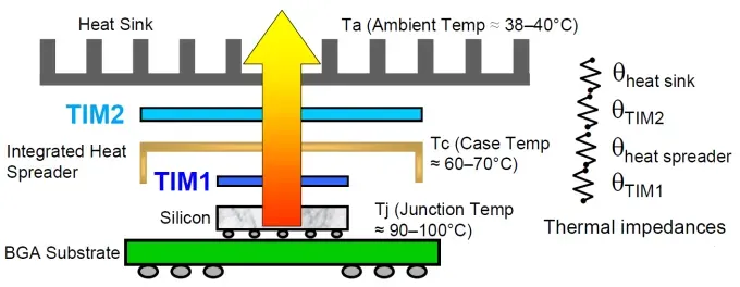
In applications handling high current or high-frequency signals, the Thermal Pad at the bottom of a QFN component plays a dual core role: "Heat Dissipation Path" and "Electrical Grounding."
From a Thermodynamic Perspective: Heat generated during chip operation must conduct through the Die Attach layer to the Thermal Pad, and then through the Solder Joint to the PCB copper foil and thermal vias. If large-area Voids occur during soldering, they not only cut off the thermal conduction path, causing the Junction Temperature (Tj) to skyrocket, but also create local Hot Spots, accelerating chip aging.
From an Electrical Perspective: The Thermal Pad is typically the reference ground (GND) for the chip. If soldering is poor or "open joints" occur, grounding impedance becomes unstable. In high-frequency operation, this leads to severe Ground Bounce effects and Electromagnetic Interference (EMI), potentially causing feedback control failure in power ICs and inducing output voltage oscillation.
For the Production Line: Reworking QFNs is an absolute "nightmare." Since the solder joints are located at the bottom of the component, they cannot be repaired directly with a soldering iron; a hot air gun or infrared rework station is required. This is time-consuming, and PCB pads are prone to lifting during secondary heating. Therefore, precise stencil and via design must be implemented during the Design for Manufacturing (DFM) stage to eliminate future troubles.
In the SMT (Surface Mount Technology) process, a common mistake made by novice engineers is designing the Thermal Pad stencil Aperture as a 1:1 full opening relative to the pad. This intuitive design leads to serious consequences in practice.
To precisely control solder volume and provide exhaust channels, the industry has developed segmented aperture techniques. According to IPC-7525 and practical experience, dividing a large pad into multiple small sections is the standard solution.
| Pad Size (mm) | Recommended Pattern | Total Aperture Ratio | Bridge Width (mm) | Expected Benefit | | :--- | :--- | :--- | :--- | :--- | | < 2.0 x 2.0 | Single Hole (No division) | 90% - 100% | N/A | Area is small, gas escapes easily; no division needed. | | 3.0 x 3.0 | Window Pane (2x2) | 50% - 60% | 0.3 - 0.4 | Balances support force, establishes exhaust channels. | | > 5.0 x 5.0 | Grid / Matrix | 50% - 60% | 0.5 | Prevents solder collapse, maximizes exhaust efficiency. |
To conduct heat away quickly, engineers usually place a matrix of Thermal Vias on the Thermal Pad. However, if these vias are handled improperly, they become the culprit for solder loss.
If vias are designed as "Through Holes" without any plugging treatment, molten solder paste will be drawn by Capillary Action during reflow, flowing down the via to the back of the PCB. This results in:
| Process Name | Description | Risks & Disadvantages | Applicable Scenario | | :--- | :--- | :--- | :--- | | Open Via | No treatment done. | Extremely high risk of solder wicking and open joints. | Only for designs where vias are off-pad. | | Tenting | Cover hole with Solder Mask. | Air trapped inside expands when heated, potentially breaking the mask (Popcorning) or forming bumps. | Low-cost consumer electronics, but low reliability. | | Plugging | Fill hole with resin/ink. | If filling is not solid, bubbles may remain; surface planarity depends on the process. | Mid-range products; surface planarity must be monitored. | | VIPPO (Type VII) | Plug, grind, and plate over. | Most complex process, but best results. | High power, high reliability, high density designs. |
Avoidance Guide: If limited by cost and unable to use VIPPO, yet vias must be placed within the pad, it is recommended to keep the via diameter below 0.3mm (12 mil). Use stencil design to avoid printing paste directly over the vias, relying on the spread of molten solder to cover the pad, thereby minimizing loss. However, for high-wattage applications, this remains a compromise.
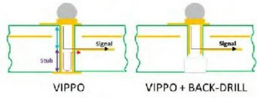
For extreme thermal dissipation demands in high-end power modules, automotive electronics, and AI servers, the VIPPO (Via-in-Pad Plated Over) technology defined by the IPC-4761 Type VII standard is the current ultimate solution. In this field, eCloud Technology has demonstrated exceptional process capabilities, becoming the preferred partner for many high-end R&D projects.
VIPPO technology involves vacuum-plugging the via with epoxy resin, curing it, performing Planarization (grinding), and then plating a Copper Cap over the hole surface. This creates a perfectly flat metal surface, enabling:
In the VIPPO process, the biggest technical barriers are "Planarization Control" and "Bonding Strength."
High Planarization Accuracy: Insufficient grinding leads to protruding copper caps, causing uneven solder paste thickness; excessive grinding causes thin caps or Dimples. eCloud Technology uses high-precision automated grinding equipment to control surface variations at the micron level, ensuring absolute flatness for QFN placement and eliminating component tilt or open joints caused by uneven pads.
IPC Class 3 Reliability: Addressing the high-reliability needs of automotive and industrial controls, eCloud Technology strictly adheres to IPC-6012 Class 3 standards. For VIPPO copper cap thickness, they ensure it meets or exceeds the required 12μm (0.47 mil), with hole wall copper thickness controlled above 25μm. This means even under severe Thermal Cycling tests, VIPPO pads produced by eCloud Technology will not suffer from Cap Separation or hole opening fractures.
Optimized Resin Matching: eCloud Technology uses specialized plugging resins with a Coefficient of Thermal Expansion (CTE) that is highly matched to the PCB substrate. This effectively solves the hidden danger of "board bursting" or copper cap lifting caused by excessive CTE differences between resin and copper during high-temperature reflow.
For Taiwanese engineers and electromechanical students pursuing extreme performance, QFN thermal optimization is not just about drawing the circuit diagram, but about a deep understanding of production processes.
When designing the next generation of high-performance products, please be sure to take these process details into account, allowing the Thermal Pad to truly perform effectively and staying far away from the nightmares of overheating and rework.
