February 10, 2026
Introduction — Manufacturing Bottlenecks in the Era of Miniaturization
In the field of contemporary electronic engineering, as semiconductor manufacturing continues to shrink according to Moore's Law, chip packaging technology is facing unprecedented density challenges. From early Dual In-line Packages (DIP) to Surface Mount Technology (SMT), and now to mainstream Ball Grid Array (BGA) and Chip Scale Packages (CSP), every iteration of technology has been accompanied by a significant reduction in pin pitch.
Driven by High-Performance Computing (HPC), 5G communication modules, and wearable biomedical monitoring devices, IC pin pitch has rapidly transitioned from the standard 1.27mm, 1.0mm, and 0.8mm to the 0.5mm and even 0.4mm fine-pitch generation.
When the pitch shrinks below 0.5mm, the difficulty of Printed Circuit Board (PCB) manufacturing rises exponentially. This is not just a reduction in geometric dimensions, but a comprehensive test of materials science, photochemical imaging, and fluid mechanics. At such a microscopic scale, the Solder Mask (commonly known as Green Oil), traditionally viewed as a secondary auxiliary material, has undergone a fundamental shift in its role. It is no longer just an insulating layer to prevent oxidation; it is a critical structural component that determines assembly yield, solder joint reliability, and final product lifespan.
In the PCB pad design for BGA packaging, a Solder Dam refers to the slender strip of solder mask ink located between two adjacent pads.
Its primary function is to establish a physical barrier during the reflow process. Utilizing the surface energy characteristics of the polymer material, it blocks the flow of molten solder, preventing Solder Bridging and short circuits caused by capillary action or surface tension imbalance.
However, as the pitch decreases, the physical space left for the solder dam is compressed to the extreme:
At this limit, the solder dam is extremely prone to fracture, peeling, or disappearing due to over-development during the PCB manufacturing process. This phenomenon, known as "Solder Dam Fracture," is currently one of the biggest technical bottlenecks in fine-pitch PCB manufacturing, second only to via processes.

According to international standards like IPC-7351 and IPC-SM-840, the design of solder dams must account for manufacturing capabilities and material properties.
| Ball Pitch | Component Type | Recommended Mask Expansion (One Side) | Recommended Min. Dam Width | Risk Level | | :--- | :--- | :--- | :--- | :--- | | > 0.8 mm | Coarse Pitch | 3 - 4 mil | ≥ 4 mil | Low | | 0.5 – 0.8 mm | Standard Pitch | 2 - 3 mil | ≥ 3–4 mil | Medium | | < 0.5 mm | Fine-pitch | 1 - 2 mil | ≥ 2–3 mil | Extremely High |
Data Source: Compiled from IPC recommendations and industry practices
As shown above, when the pitch is less than 0.5mm, to maintain insulation between pads, the design width of the solder dam is forced to compress to 2-3mil (approx. 50-75 μm). This approaches the material limit of Liquid Photoimageable Solder Mask (LPI).
The bonding of the solder mask to the copper surface or substrate (FR-4) relies primarily on two mechanisms: chemical bonding and Mechanical Interlocking. When the solder dam width shrinks below 75 μm, its contact area with the substrate ($A_{contact}$) decreases drastically. According to adhesion mechanics:
$$ F_{adhesion} = \tau \times A_{contact} $$
Where $F_{adhesion}$ is the total adhesion force, and $\tau$ is the shear adhesive strength of the material. When $A_{contact}$ approaches a minimum value, external stresses encountered during the process (such as high-pressure developer sprays or thermal stress during curing) can easily exceed $F_{adhesion}$, causing the solder dam to peel off the substrate.
Another major cause of solder dam fracture comes from the "Side Erosion" or "Undercut" effect during the photochemical process. When using Sodium Carbonate (Na₂CO₃) solution for development, the developer not only dissolves the unexposed areas but also erodes the edges of the exposed, cured areas from the side.
On a microscopic 3mil dam, a side erosion of 0.5mil on each side means the effective adhesion width may only remain 2mil or less. This "narrow waist" structure breaks easily under fluid impact, forming "Solder Mask Slivers," which become potential breeding grounds for short circuits.
Facing the physical limits of 0.5mm Pitch, design engineers must choose between two pad definition methods: Non-Solder Mask Defined (NSMD) and Solder Mask Defined (SMD).
In NSMD design, the solder mask opening is larger than the copper pad size.
In SMD design, the solder mask covers the edges of the copper pad.

| Comparison Item | NSMD (Copper Defined) | SMD (Mask Defined) | 0.5mm Pitch Recommendation | | :--- | :--- | :--- | :--- | | Solder Joint Strength (Thermal) | Excellent (Stress Dispersion) | Poor (Stress Concentration) | For Industrial/Server Products | | Solder Joint Strength (Mechanical) | Poor (Prone to Pad Cratering) | Excellent (Mask Anchoring) | For Mobile/Wearable Devices | | Dimensional Precision | High (Controlled by Etching) | Low (Controlled by Mask Alignment) | NSMD Preferred | | Solder Bridge Risk | Higher (No mask isolating edges) | Lower (Mask limits flow) | Requires High-Quality Solder Dams |
For 0.5mm Pitch, IPC and most chip manufacturers (e.g., TI, ADI) typically recommend NSMD, but this is predicated on the Solder Dam remaining intact.
Solder bridging is the most fatal defect in fine-pitch assembly. According to the Young-Laplace equation:
$$ P_{int} = P_{ext} + \gamma \left( \frac{1}{R_1} + \frac{1}{R_2} \right) $$
At 0.5mm Pitch, without the physical barrier of a solder dam, if Over-wetting occurs or if there is excessive solder paste volume, the liquid solder droplets will attempt to reach equilibrium by minimizing surface energy, leading to an instantaneous short circuit.
Facing the physical limits imposed by 0.5mm Pitch, traditional film exposure processes are no longer sufficient. The electronics manufacturing industry is shifting entirely toward digital lithography technology—Laser Direct Imaging (LDI).
LDI technology eliminates photographic film, using high-power UV lasers combined with Digital Micromirror Devices (DMD) to image CAD data directly onto the PCB.
In the high-precision PCB manufacturing and assembly supply chain, eCloud Technology addresses the stringent requirements for 0.5mm Pitch BGA projects by decisively adopting high-end LDI exposure systems, delivering the following value:
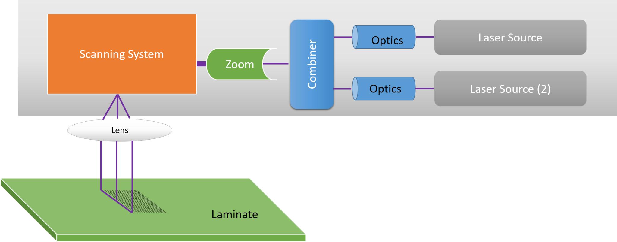
The challenge of W9-0.5mm Pitch is essentially a game between physical limits and manufacturing craftsmanship. From the fracture analysis of physical mechanics to the design trade-off between NSMD and SMD, the answer ultimately returns to "Precision."
eCloud Technology utilizes LDI technology to overcome material physical limits with photon-level precision. This provides a textbook example for RD engineers: "In extreme manufacturing, only extreme precision can achieve reliable quality."
About the Author Ben Ho is the Business Development Manager at eCloud Technology, specializing in high-end PCB manufacturing processes and electronic assembly solutions.
Is your project facing fine-pitch design challenges? Contact us for a DFM consultation.
