1. Core Technology: Demystifying Drilling for R&D Engineers
In PCB cost structures, drilling expenses often account for 30% to 40% of the total cost. While many R&D engineers know the rules of thumb that "smaller holes are more expensive" and "thicker boards are harder to drill," few delve into the underlying physical and mechanical limitations.
1.1 Why are "Smaller Holes More Expensive"?
Mechanical Drilling is a process that uses a Tungsten Carbide drill bit rotating at high speed to remove substrate material. When the drill diameter shrinks below 0.2mm, the cost structure undergoes a qualitative change, primarily constrained by the following three physical factors:
-
Drill Bit Lifespan and Breakage Risk
Standard-sized drill bits (e.g., above 0.3mm) have stronger rigidity and can typically withstand over 15,000 hits. However, for micro-vias (e.g., 0.15mm or 0.1mm), the drill bits are extremely prone to breakage due to run-out or stress. Data shows the lifespan of micro-drill bits plummets, often requiring replacement after only 3,000 to 5,000 hits. Frequent tool changes not only increase consumable costs but also significantly reduce machine utilization efficiency.
-
Limitations on Stack Height
To improve efficiency, multiple boards are typically stacked and drilled through at once during mass production. For 0.2mm holes, a factory might stack 3 to 4 panels for processing. But for 0.1mm micro-vias, to prevent drill bit wander causing misalignment in lower layers, often only single-panel stacking (1-panel stack) can be used. This means output plummets by 60% to 70% for the same machine time, which is the root cause of the soaring cost for small-diameter drilling.
-
Processing Efficiency and RPM
Micro-via machining requires extremely high rotational speeds (150k - 300k RPM) to maintain cutting speed, but the in-feed rate must be slowed to prevent breakage. Compared to laser drilling which can achieve speeds of up to 150 holes per second, mechanical drilling faces significant efficiency bottlenecks in the micro-via domain.
1.2 Why are "Thicker Boards Harder to Drill"?
Increased board thickness primarily presents challenges in "Chip Evacuation" and "Heat Accumulation."
- Difficulty in Chip Evacuation: During deep hole drilling, resin and glass fiber debris within the drill bit's flutes are difficult to expel. If debris clogs, frictional heat can cause Resin Smear, forming an insulating layer on the hole wall that hinders subsequent copper plating for electrical connection.
- Amplification of Run-out: Drill bits have minimal flexibility; the deeper the hole, the greater the wobble amplitude of the drill tip at the hole bottom. This can lead to hole misalignment from the pad center or even drilling through inner layer traces.
Table 1: Mechanical Drilling vs. Laser Drilling Characteristics Comparison
| Characteristic | Mechanical Drilling | Laser Drilling |
| :--- | :--- | :--- |
| Applicable Hole Diameter | > 0.15mm (Through-hole/Blind & Buried) | < 0.15mm (Micro-blind via) |
| Machining Mechanism | Cutting (Contact) | Ablation (Non-contact) |
| Aspect Ratio Limit | Can reach 10:1 (or higher) | Limited to 0.75:1 ~ 1:1 |
| Primary Cost Driver | Drill Bit Wear, Low Stack Height | Machine Depreciation, Process Steps |
| Hole Shape | Cylindrical | Inverted Trapezoid (V-shape) |
2. Cost Threshold: The Price Ladder of Aspect Ratio (AR)
Aspect Ratio (AR) is defined as the ratio of board thickness to drill hole diameter:
AR = Board Thickness / Drill Hole Diameter
The AR value not only affects drilling difficulty but also directly determines the yield of "Plating". Plating solution must rely on capillary action and fluid dynamics to enter the hole. The higher the AR, the more difficult the solution exchange, easily leading to the "Dog-bone Effect" — excessive copper thickness at the hole mouth and insufficient thickness at the hole center, posing reliability risks.
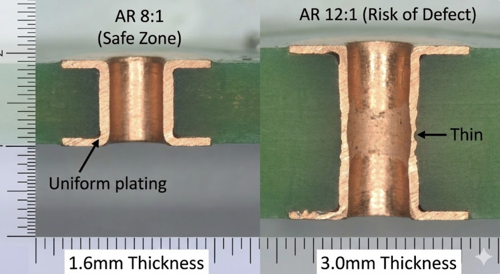
2.1 AR 8:1 —— The Cost Sweet Spot (Safe Zone)
- Definition: e.g., 1.6mm board thickness with 0.2mm hole diameter.
- Cost Impact: This is the comfort zone for standard processes. Most PCB manufacturers' standard equipment can achieve good hole wall plating throwing power without special parameters. Within this range, R&D engineers get the most competitive quotes with no additional charges.
2.2 AR 10:1 —— The Warning Line
- Definition: e.g., 2.0mm board thickness with 0.2mm hole diameter, or 3.0mm board thickness with 0.3mm hole diameter.
- Cost Impact: Entering this range, yield begins to decline. The plating process needs reduced current density and extended time to ensure copper thickness meets standards in deep holes. Drill breakage risk increases during drilling. This typically triggers a 10% to 20% cost adder.
- Design Suggestion: Unless space is absolutely constrained, it's recommended to increase the hole diameter to return to the 8:1 zone.
2.3 AR 12:1 and Above —— The Turning Point to Abandon Mechanical Drilling
- Definition: e.g., Backplanes or server boards above 3.2mm attempting to use 0.25mm through-holes.
- Technical Bottleneck: At this point, the deviation of mechanical drilling may exceed the safety margin of the pad, and the throwing power of traditional DC Plating will drop below 60%,极易造成孔内开极易 causing opens within the hole.
- Decision Point: When design requirements force AR beyond 12:1, persisting with traditional through-holes will lead to exponentially rising costs and questionable reliability. At this stage, switching to HDI technology is often a better choice. By decomposing one deep through-hole into multiple low-aspect-ratio blind and buried vias (e.g., 1-step or 2-step HDI), it not only solves plating issues but also releases inner layer routing space.
3. Layout Guidelines: Timing for HDI Layer Selection and Its Routing Advantages
HDI (High-Density Interconnect) achieves micro-via connections through laser drilling and build-up methods. Although HDI increases lamination cycles, its overall benefits often outweigh traditional processes for high-density BGA fan-out.
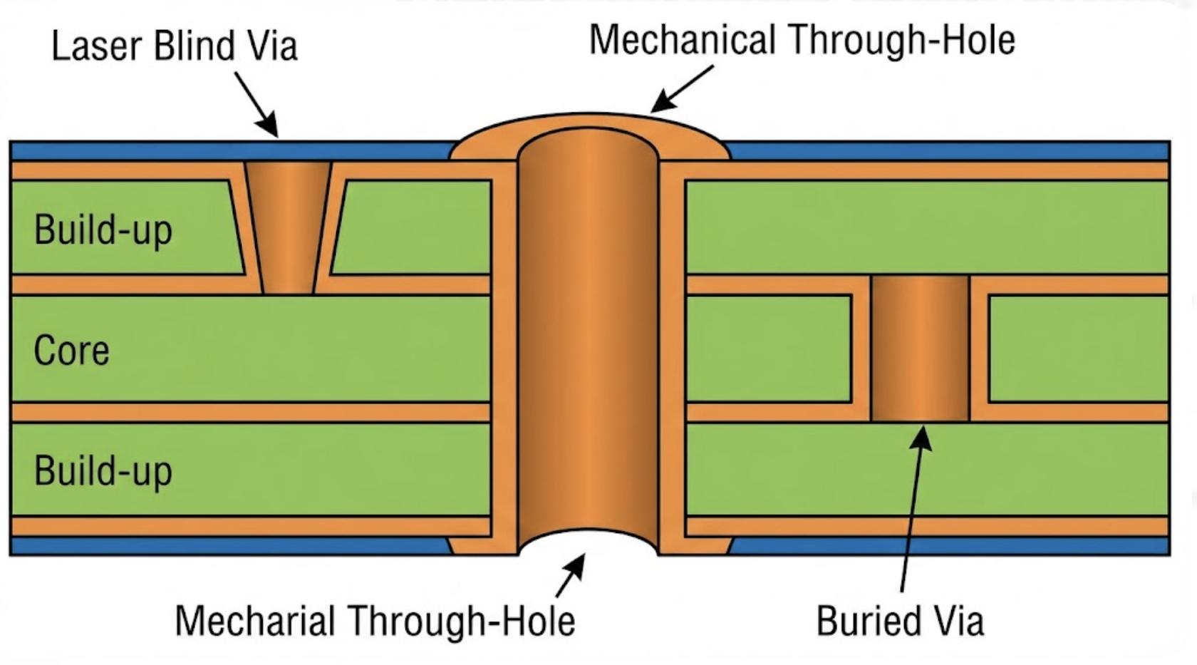
3.1 1-step HDI (1+N+1): The Cost-Effective Choice
- Structure: One build-up layer on each side of the core layer, containing "Laser Blind Vias" and "Mechanical Through-Holes/Buried Vias."
- When to Choose: When the ball pitch of the main chip BGA shrinks to 0.5mm. At this point, traditional through-hole pads can no longer route traces between solder balls, necessitating Via-in-Pad technology. The laser micro-vias of 1-step HDI (typically 0.1mm) can be drilled directly on the BGA pad, eliminating the need for dog-bone fan-out and greatly saving space.
- Routing Advantage: Blind vias do not penetrate the entire board, so the inner layers directly below them can form complete "Boulevards" for routing, providing 2 to 3 times more routing channels than through-hole boards. This is especially suitable for routing high-speed parallel buses like DDR4/DDR5.
3.2 2-step HDI (2+N+2): The Price of Ultimate Density
- Structure: Adds another lamination and laser drilling cycle on top of the 1-step structure.
- When to Choose: When BGA pitch reaches 0.4mm or smaller, and I/O count is extremely high.
- Staggered vs. Stacked Vias:
- Staggered: The upper and lower micro-vias do not overlap. Process is simpler, cost is lower.
- Stacked: Micro-vias are vertically stacked. This requires "Copper Filling" and planarization of the lower via before drilling the second layer via on top. This process is extremely expensive, typically increasing cost by 20% to 30%+ compared to 1-step HDI.
- Cost Red Line: Unless absolutely necessary (e.g., smartphone motherboards or ultra-high-density modules), avoid using 2-step HDI with stacked via structures.
Table 2: HDI Layer Count Cost vs. Capability Comparison
| HDI Layer Count | Applicable BGA Pitch | Relative Cost Index | Routing Capability | Key Process |
| :--- | :--- | :--- | :--- | :--- |
| Traditional Through-Hole | > 0.65mm | 100 | Low | Mechanical Drilling |
| 1-step (1+N+1) | 0.5mm | 140 - 160 | Medium-High | Laser Drilling, Via-in-Pad |
| 2-step (2+N+2) | <= 0.4mm | 180 - 220 | Very High | Filled Via Plating, Secondary Lamination |
4. Showcasing Expertise: eCloud Technology's Deep-Hole Plating Capability for High Aspect Ratio Server Boards
In high-end servers, AI computing units, and 5G communication backplanes, PCB layer counts often exceed 20 layers, with board thickness reaching 3.0mm or more. Under these extreme conditions, aspect ratios frequently break 15:1 or even 20:1. This is beyond the capability of standard HDI or processes and requires special "Deep Hole Process" capabilities.
The manufacturing pain point for such high-end boards is: how to uniformly plate sufficient copper thickness (typically 25μm per IPC Class 3 requirement) inside extremely deep and narrow holes, while avoiding excessive plating at the hole mouth causing trace shorts?
4.1 Periodic Pulse Reverse (PPR) Plating Technology
Traditional DC Plating has very poor throwing power in high AR holes. eCloud Technology employs advanced PPR plating technology when handling such high aspect ratio orders.
- Mechanism: PPR uses forward current to deposit copper and periodically applies a brief high-current "reverse pulse." This reverse pulse preferentially dissolves the excess copper ions at the hole mouth (high current density area), thereby "peaking and filling valleys," forcing copper ions to move more effectively towards the hole center.
- Effectiveness: Under extreme conditions of AR 20:1, PPR technology can improve deep-hole throwing power from 60% with DC to over 85% - 90%, ensuring the copper thickness at the hole center meets stringent IPC Class 3 specifications and eliminating hidden opens.
4.2 The Bane of High-Speed Signals: Backdrilling
If through-holes on server boards have excess unused portions (Stub), they act as antennas at high frequencies (e.g., PCIe Gen5, 112G SerDes), causing severe signal reflection.
- Process Capability: eCloud Technology possesses high-precision backdrilling capability (Controlled Depth Drilling), able to drill away the unused via barrel from the board backside.
- Precision Requirement: To maximize signal integrity, the residual stub length after backdrilling must be controlled within 10 mils (0.25mm), even challenging the 5 mil limit. This requires extremely high-precision Z-axis control machines to avoid damaging inner layer functional traces, a key indicator distinguishing high-end from low-end PCB manufacturers.

4.3 eCloud Technology's Technical Positioning
Addressing the needs of Taiwanese engineers developing AI servers, high-end switches, and similar products, eCloud Technology integrates a one-stop process from high-precision mechanical drilling, advanced HDI laser drilling, to deep-hole pulse plating. Especially for the challenge of High Aspect Ratio, through optimized plating chemistry and PPR parameters, it solves the physical难题 of "difficult plating in thick boards," providing R&D with a reliable solution balancing cost and performance.
Conclusion
PCB via design is an art of "trade-offs." Every via an engineer draws in Layout silently calculates cost.
- Hold the 8:1 Sweet Spot: In general designs, try to keep the aspect ratio within 8:1. This is the golden rule for ensuring low cost and high yield.
- Choose HDI Rationally: When BGA pitch is below 0.5mm or through-hole AR exceeds 12:1, decisively adopt 1-step HDI. Although unit price increases, the resulting routing advantages and yield improvement often reduce overall system cost.
- Value Deep-Hole Capability: For thick-board server designs, drilling and plating are lifelines for quality. Choosing a partner with PPR plating and high-precision backdrilling capabilities (like eCloud Technology) is a necessary investment to ensure products pass rigorous signal testing and reliability validation.
Understanding these underlying logics allows R&D engineers to drill the true "cost sweet spot" for their company on the design drawings.
