June 16, 2026
In the design field of EV inverters, AI server power modules, industrial frequency converters, and energy storage systems, "the board works perfectly in the lab but dies shortly after field deployment" is a nightmare almost every power engineer has faced. When high current surges through the copper foil, the PCB simultaneously endures the pulling of three forces: thermal, electrical, and mechanical stress. If any of these defense lines are breached, the entire circuit board may suffer cascading failures within months of mass production. This article breaks away from the traditional format of simply listing "failure modes." Starting from controllable engineering variables on the design side, we will dismantle the three major failure paths of high-power PCBs one by one and provide design guidelines that can be directly applied during the prototyping and mass production stages.
Once a high‑power PCB begins operation, the physical phenomenon of P = I²R kicks in immediately. What is even trickier is that the temperature coefficient of resistance for copper is approximately 0.39%/°C. Temperature rises → resistance increases → heat generation rises further, forming a positive feedback loop known as the “thermal runaway spiral.” If this cycle is not effectively suppressed, it will trigger three typical failures.
Many engineers still habituate to assigning trace widths based on experience. This works for low‑to‑medium power, but severe problems arise at 50 A and above. Recommended engineering practices:
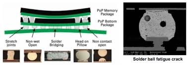
Automotive, aerospace, and industrial equipment easily experience hundreds of temperature cycles daily. With every thermal fluctuation, solder joints undergo minute thermal expansion and contraction. Intermetallic compounds (IMC) gradually crystallise and grow, eventually leading to cracks extending from stress concentration points.
To mitigate solder joint fatigue risks, pay attention during the design phase:
If the heat from power components like MOSFETs, IGBTs, and DC‑DC modules cannot be efficiently conducted away, junction temperatures exceeding the limit is only a matter of time. Common practical techniques to enhance thermal design:
As for delamination, this historic problem is particularly prone to occur in heavy copper and high‑temperature scenarios. The logic for selecting Tg (Glass Transition Temperature) should be:
| Operating Temperature Range | Recommended Substrate Direction | | :--- | :--- | | < 100 °C | Standard FR‑4 (Tg ≥ 130 °C) is sufficient | | 100 – 130 °C | Upgrade to High‑Tg FR‑4 (Tg ≥ 170 °C) | | > 130 °C | Switch to Polyimide or Metal Core PCB (MCPCB) |
Engineering Rule of Thumb: Tg should be at least 20 °C – 25 °C higher than the actual operating temperature, strictly avoiding long‑term operation right at the Tg threshold.
When voltages are pulled up to hundreds of volts or even kV levels, the risk of electric field breakdown hides between every trace, every via, and every copper plane. Such failures are often only exposed during high‑temperature and high‑humidity testing in the lab, remaining invisible in the early stages of mass production, making them extremely tricky to catch.
Creepage and clearance are two entirely distinct concepts. Clearance is the shortest distance through the air, while creepage is the shortest path along the insulating surface. When designing, be sure to note:
Many treat voltage drop as purely an efficiency issue, but in high‑power applications, voltage drop directly equates to heat generation. A standard criterion: If the rail voltage drop exceeds 1% – 2% of the power rail’s nominal voltage, the conductor’s cross‑sectional area must be increased, or busbars should be adopted.
CAF (Conductive Anodic Filament) is a conductive filament formed by the migration of copper ions along the interface between the resin and glass fibre within the PCB weave structure. Its terror lies in:
Key Preventions:
Partial Discharge occurs in microscopic voids or interface defects within insulating materials and progressively degrades the insulation layer over time. Avoiding sharp conductor corners, utilising 45° chamfers or arc routing, and requiring manufacturers to use void‑free prepreg are critical preventative measures on the design side.
Under environments subjected to heavy copper, thick boards, massive connectors, and intense vibrations, the PCB’s physical structure bears immense pressure. Mechanical failure is often not overlooked during design, but rather vastly underestimated.
High‑power designs naturally necessitate thicker copper, higher layer counts, and greater board thicknesses, which in turn drastically pushes up the via’s aspect ratio. When the aspect ratio exceeds 10:1, the via becomes highly susceptible to wall cracking during the plating process, subsequent reflow thermal shocks, and within vibration‑heavy environments.
Design Guidelines:
When copper thickness distribution is severely imbalanced along the Z‑axis, the board will inherently bend during reflow—much like a sandwich heated unevenly. Subsequent cascading impacts include BGA solder joint open circuits, fractured ceramic components, and boards catastrophically jamming in PCBA test fixtures.
Design and Prototyping Guidelines to Prevent Warpage:
The aggressive vibration environments inherent in automotive and heavy industrial equipment act as invisible PCB assassins. What must be contemplated during design is not simply “can the board fit inside the enclosure,” but “will the board still be fully functional after 10 years and 100,000 kilometres.”
Practical Approaches:
High‑power PCB failures are never the result of a single isolated cause; they are the consequence of the long‑term, compounding interaction of three distinct stress fields: thermal, electrical, and mechanical. A truly reliable high‑power board inevitably stems from:
Investing a week to meticulously figure out these details before mass production is exponentially cheaper than executing customer complaint failure analysis after the fact. For R&D teams actively diving into high‑power applications—such as AI server power supplies, EV powertrains, and heavy industrial power systems—discipline during the design phase is the ultimate insurance for long‑term reliability.
